
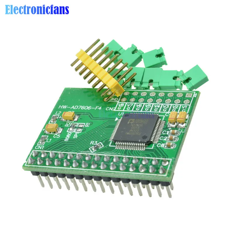
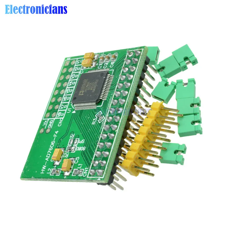
16Bits ADC 8CH Synchronization AD7606 DATA Acquisition Module 200Ksps


16Bits ADC 8CH Synchronization AD7606 DATA Acquisition Module 200Ksps
SKU:011006
Regular price
$18.99
![]()
- guaranteeQuality checked
- Special gift cardsSpecial gift cards
- Free return Within 60 days
- Consultancy86-0755-85201155
![]()
Tip : To facilitate your choice , PCB board analog input front -row pin (2x8/2.54mm pitch ) default not weld .
We will be giving away 2x8 's double needle and eight jumpers from the customer's own choice is up welding, soldering or down .
1, using high-precision 16-bit ADC chip AD7606
2,8 analog inputs. 1M ohm impedance.[No negative supply, there is no front-end analog amplifier can be connected directly to the sensor output]
3, the input range of plus or minus 5V, plus or minus 10V. By IO control.
4, Resolution 16.
5, the maximum sampling frequency sampling rate of 200ksps.
Supports eight sampling settings file (which can effectively reduce the jitter)
6, built-in benchmark
7, a single 5V power supply
8, SPI Interface, or 16-bit bus interface. Interface IO level can be 5V or 3.3V.
6, built-in benchmark
7, a single 5V power supply
8, SPI Interface, or 16-bit bus interface. Interface IO level can be 5V or 3.3V.
We AD7606 module factory default is 8080 parallel interface.
If SPI interface mode, you need to modify R1 R2 resistor configuration.
Parallel Mode Jumper: R1 floating (not stickers), R2 10K resistor paste
SPI interface mode jumper: R1 stickers 10K resistor, R2 floating (not stickers)
AD7606 configuration is very simple, it has no internal registers.
If SPI interface mode, you need to modify R1 R2 resistor configuration.
Parallel Mode Jumper: R1 floating (not stickers), R2 10K resistor paste
SPI interface mode jumper: R1 stickers 10K resistor, R2 floating (not stickers)
AD7606 configuration is very simple, it has no internal registers.
Range and over-sampling parameters are controlled via an external IO.
Pulse frequency sampling rate provided by the microcontroller or DSP control.
AD7606 must use a single 5V supply.
Level communication interface between the AD7606 and SCM controlled by VIO pin.
That VIO power supply must be connected to the microcontroller can be 3.3V can also be 5V.Pulse frequency sampling rate provided by the microcontroller or DSP control.
AD7606 must use a single 5V supply.
Level communication interface between the AD7606 and SCM controlled by VIO pin.
[Module Pin Description]
OS2 OS1 OS2: a combination of state selection oversampling mode.
000 means no oversampling, the maximum sampling rate of 200ksps.
001 represents two times oversampling, which is the hardware inside collected two samples averaging
010 represents four times oversampling, which is the hardware inside collect four samples averaged
011 represents eight times oversampling, which is the hardware inside collected eight samples averaged
100 represents 16 times oversampling, which is the hardware inside collected 16 samples averaged
101 represents 32 times oversampling, which is an internal hardware averaging collected 32 samples
110 represents 64 times oversampling, which is the hardware inside collected 64 samples averaged
Oversampling ratio is higher, the longer the ADC conversion time, the lower the maximum sampling frequency can be obtained.
CVA, CVB: AD conversion start control signal channel 1-4 decision CVA, CVB decided 5-8 channels.
Two signals can stagger a short time, in general, can be CVA, CVB parallel together.
RAGE: Select the range of 0 means plus or minus 5V, 1 indicates negative 10V.
RD: Read signal
RST: Reset signal
Busy: Busy Signal
CS: chip-select signal
FRST: first a channel samples indicating signal
VIO: communication interface level
DB0 - DB15: Data Bus
[16 parallel mode wiring diagram --- AD7606 also supports 8-bit bus mode, see the AD7606 data sheet
MCU side AD7606 module
GND <----- ground
+5 V <----- 5V power supply
RAGE <----- can also be connected to the GPIO connected fixed level
OS2 <----- can also be connected to the GPIO connected fixed level
OS1 <----- can also be connected to the GPIO connected fixed level
OS0 <----- can also be connected to the GPIO connected fixed level
CVA <----- access the GPIO (output) is used to start AD conversion [Recommended pick pin with PWM output capability]
CVB <--- |
RD <----- 8080 bus read signal NOE
RST <----- GPIO output hardware reset AD606
Busy -----> GPIO input AD606 being converted instructions. [Recommended connection with external pin interrupt capability]
CS <----- 8080 bus chip select NCS
VIO <----- microcontroller power supply
DB0-DB15 -----> 8080 data bus (16)
FRST may take
[SPI interface mode wiring diagram
MCU side AD7606 module
GND <----- ground
+5 V <----- 5V power supply
RAGE <----- any output GPIO, can be accessed by a fixed level
OS2 <----- any output GPIO, can be accessed by a fixed level
OS1 <----- any output GPIO, can be accessed by a fixed level
OS0 <----- any output GPIO, can be accessed by a fixed level
CVA <----- access the GPIO (output) is used to start AD conversion [Recommended pick pin with PWM output capability]
CVB <--- |
RD / SCLK <----- SPI bus clock SCK
RST <----- any output GPIO, for hardware reset AD606
Busy -----> GPIO input, AD606 being converted instructions. [Recommended connection with external pin interrupt capability]
CS <----- SPI bus chip select SCS
VIO <----- microcontroller power supply
DB7 (DOUTA) -----> SPI bus data lines MISO
DB14 - DB15 may pick
FRST may take
Software implementations [1] --- timing acquisition of SPI example we offer document using this program, see bsp_spi_ad7606.c
In the timer interrupt service routine implementation:
Timer interrupt ISR:
{
Interrupt entry;
8 reads the sampling results are stored in the RAM channel; ----> read is the last record collection for continuous acquisition, it is not related to the
Start next ADC acquisition; (flip CVA and CVB)
Interrupt return;
}
Timer frequency is the ADC sampling frequency. This mode can not connect busy port cable.
Software implementations [2] --- timed 8080 acquisition of the interface we provide an example of using this program, see bsp_ad7606.c file
Configure CVA CVB pin PWM output mode, the sampling period is set to the desired frequency; ---> After the MCU will produce a very stable AD conversion cycle signal
The busy port line is set to interrupt falling edge trigger mode;
External interrupt ISR
{
Interrupt entry;
8 reads the sampling results of the channel stored in the RAM;
Interrupt return;
}
[1 and 2, the differences in implementations of software-timed acquisition]
(1) Option 1 may be less busy lines, but the other main interrupt service routine or temporary closure of the global interrupt when ADC conversion cycle may cause a slight jitter.
(2) Option 2 can ensure the stability of the acquisition of the clock, because it is generated by the MCU hardware, but need more then a BUSY mouth lines.
Package included:
- 1 PCS x 16Bits ADC 8CH Synchronization AD7606 DATA Acquisition Module 200Ksps
![]()


![]()
7868
HOT SELLING
 |
 |
 |
 |
 |
 |
 |
 |
 |
 |
 |
 |
 |
 |
 |
 |
 |
 |
 |
 |
Purchasing & Delivery
Before you make your purchase, it’s helpful to know the measurements of the area you plan to place the furniture. You should also measure any doorways and hallways through which the furniture will pass to get to its final destination.Picking up at the store
Shopify Shop requires that all products are properly inspected BEFORE you take it home to insure there are no surprises. Our team is happy to open all packages and will assist in the inspection process. We will then reseal packages for safe transport. We encourage all customers to bring furniture pads or blankets to protect the items during transport as well as rope or tie downs. Shopify Shop will not be responsible for damage that occurs after leaving the store or during transit. It is the purchaser’s responsibility to make sure the correct items are picked up and in good condition.Delivery
Customers are able to pick the next available delivery day that best fits their schedule. However, to route stops as efficiently as possible, Shopify Shop will provide the time frame. Customers will not be able to choose a time. You will be notified in advance of your scheduled time frame. Please make sure that a responsible adult (18 years or older) will be home at that time.In preparation for your delivery, please remove existing furniture, pictures, mirrors, accessories, etc. to prevent damages. Also insure that the area where you would like your furniture placed is clear of any old furniture and any other items that may obstruct the passageway of the delivery team. Shopify Shop will deliver, assemble, and set-up your new furniture purchase and remove all packing materials from your home. Our delivery crews are not permitted to move your existing furniture or other household items. Delivery personnel will attempt to deliver the purchased items in a safe and controlled manner but will not attempt to place furniture if they feel it will result in damage to the product or your home. Delivery personnel are unable to remove doors, hoist furniture or carry furniture up more than 3 flights of stairs. An elevator must be available for deliveries to the 4th floor and above.
Other Customers also buy:
-
 Translation missing: en.products.product.regular_price $5.99{"id":4417205076039,"title":"16Bits ADC 8CH Synchronization AD7606 DATA Acquisition Module 200Ksps","handle":"16bits-adc-8ch-synchronization-ad7606-data-acquisition-module-200ksps","description":"\u003cdiv\u003e\n\u003cwidget data-widget-type=\"customText\" id=\"33484937\" title=\"010166\" type=\"custom\"\u003e\u003c\/widget\u003e \r \u003cp\u003e \u003c\/p\u003e \r \u003cp\u003e \u003c\/p\u003e \r \u003cp\u003e \u003cimg alt=\"HTB1ZYSui4PI8KJjSspoq6x6MFXaU\" height=\"40\" src=\"https:\/\/ae01.alicdn.com\/kf\/HTB1ZYSui4PI8KJjSspoq6x6MFXaU.jpg\" width=\"950\"\u003e\u003c\/p\u003e \r \u003cp\u003e \u003c\/p\u003e \r \u003cdiv\u003e \r \u003cdiv\u003e \r \u003cdiv\u003e \r \u003cspan style=\"font-size: 20.0px;\"\u003e\u003cspan style=\"font-family: trebuchet ms , helvetica , sans-serif;\"\u003eTip : To facilitate your choice , PCB board analog input front -row pin (2x8\/2.54mm pitch ) default not weld .\u003c\/span\u003e\u003c\/span\u003e \r \u003c\/div\u003e \r \u003cdiv\u003e \r \u003cspan style=\"font-size: 20.0px;\"\u003e\u003cspan style=\"font-family: trebuchet ms , helvetica , sans-serif;\"\u003eWe will be giving away 2x8 's double needle and eight jumpers from the customer's own choice is up welding, soldering or down .\u003cbr\u003e \u003cbr\u003e 1, using high-precision 16-bit ADC chip AD7606\u003cbr\u003e \u003cbr\u003e 2,8 analog inputs. 1M ohm impedance.[No negative supply, there is no front-end analog amplifier can be connected directly to the sensor output]\u003cbr\u003e \u003cbr\u003e 3, the input range of plus or minus 5V, plus or minus 10V. By IO control.\u003cbr\u003e \u003cbr\u003e 4, Resolution 16.\u003cbr\u003e \u003cbr\u003e 5, the maximum sampling frequency sampling rate of 200ksps.\u003c\/span\u003e\u003c\/span\u003e \r \u003c\/div\u003e \r \u003cdiv\u003e \r \u003cspan style=\"font-size: 20.0px;\"\u003e\u003cspan style=\"font-family: trebuchet ms , helvetica , sans-serif;\"\u003eSupports eight sampling settings file (which can effectively reduce the jitter)\u003cbr\u003e \u003cbr\u003e 6, built-in benchmark\u003cbr\u003e \u003cbr\u003e 7, a single 5V power supply\u003cbr\u003e \u003cbr\u003e 8, SPI Interface, or 16-bit bus interface. Interface IO level can be 5V or 3.3V.\u003c\/span\u003e\u003c\/span\u003e \r \u003c\/div\u003e \r \u003cdiv\u003e \r \u003cspan style=\"font-size: 20.0px;\"\u003e\u003cspan style=\"font-family: trebuchet ms , helvetica , sans-serif;\"\u003eWe AD7606 module factory default is 8080 parallel interface.\u003cbr\u003e If SPI interface mode, you need to modify R1 R2 resistor configuration.\u003cbr\u003e \u003cbr\u003e Parallel Mode Jumper: R1 floating (not stickers), R2 10K resistor paste\u003cbr\u003e SPI interface mode jumper: R1 stickers 10K resistor, R2 floating (not stickers)\u003cbr\u003e \u003cbr\u003e \u003cbr\u003e AD7606 configuration is very simple, it has no internal registers.\u003c\/span\u003e\u003c\/span\u003e \r \u003c\/div\u003e \r \u003cdiv\u003e \r \u003cspan style=\"font-size: 20.0px;\"\u003e\u003cspan style=\"font-family: trebuchet ms , helvetica , sans-serif;\"\u003eRange and over-sampling parameters are controlled via an external IO.\u003cbr\u003e Pulse frequency sampling rate provided by the microcontroller or DSP control.\u003cbr\u003e \u003cbr\u003e \u003cbr\u003e AD7606 must use a single 5V supply.\u003cbr\u003e Level communication interface between the AD7606 and SCM controlled by VIO pin.\u003c\/span\u003e\u003c\/span\u003e \r \u003c\/div\u003e \r \u003cspan style=\"font-size: 20.0px;\"\u003e\u003cspan style=\"font-family: trebuchet ms , helvetica , sans-serif;\"\u003eThat VIO power supply must be connected to the microcontroller can be 3.3V can also be 5V.\u003cbr\u003e \u003cbr\u003e [Module Pin Description]\u003cbr\u003e \u003cbr\u003e OS2 OS1 OS2: a combination of state selection oversampling mode.\u003cbr\u003e \u003cbr\u003e 000 means no oversampling, the maximum sampling rate of 200ksps.\u003cbr\u003e \u003cbr\u003e 001 represents two times oversampling, which is the hardware inside collected two samples averaging\u003cbr\u003e \u003cbr\u003e 010 represents four times oversampling, which is the hardware inside collect four samples averaged\u003cbr\u003e \u003cbr\u003e 011 represents eight times oversampling, which is the hardware inside collected eight samples averaged\u003cbr\u003e \u003cbr\u003e 100 represents 16 times oversampling, which is the hardware inside collected 16 samples averaged\u003cbr\u003e \u003cbr\u003e 101 represents 32 times oversampling, which is an internal hardware averaging collected 32 samples\u003cbr\u003e \u003cbr\u003e 110 represents 64 times oversampling, which is the hardware inside collected 64 samples averaged\u003cbr\u003e \u003cbr\u003e \u003cbr\u003e Oversampling ratio is higher, the longer the ADC conversion time, the lower the maximum sampling frequency can be obtained.\u003cbr\u003e \u003cbr\u003e \u003cbr\u003e CVA, CVB: AD conversion start control signal channel 1-4 decision CVA, CVB decided 5-8 channels.\u003cbr\u003e \u003cbr\u003e Two signals can stagger a short time, in general, can be CVA, CVB parallel together.\u003cbr\u003e \u003cbr\u003e \u003cbr\u003e RAGE: Select the range of 0 means plus or minus 5V, 1 indicates negative 10V.\u003cbr\u003e \u003cbr\u003e RD: Read signal\u003cbr\u003e \u003cbr\u003e RST: Reset signal\u003cbr\u003e \u003cbr\u003e Busy: Busy Signal\u003cbr\u003e \u003cbr\u003e CS: chip-select signal\u003cbr\u003e \u003cbr\u003e FRST: first a channel samples indicating signal\u003cbr\u003e \u003cbr\u003e VIO: communication interface level\u003cbr\u003e \u003cbr\u003e DB0 - DB15: Data Bus\u003cbr\u003e \u003cbr\u003e \u003cbr\u003e [16 parallel mode wiring diagram --- AD7606 also supports 8-bit bus mode, see the AD7606 data sheet\u003cbr\u003e \u003cbr\u003e MCU side AD7606 module\u003cbr\u003e \u003cbr\u003e GND \u0026lt;----- ground\u003cbr\u003e \u003cbr\u003e +5 V \u0026lt;----- 5V power supply\u003cbr\u003e \u003cbr\u003e RAGE \u0026lt;----- can also be connected to the GPIO connected fixed level\u003cbr\u003e \u003cbr\u003e OS2 \u0026lt;----- can also be connected to the GPIO connected fixed level\u003cbr\u003e \u003cbr\u003e OS1 \u0026lt;----- can also be connected to the GPIO connected fixed level\u003cbr\u003e \u003cbr\u003e OS0 \u0026lt;----- can also be connected to the GPIO connected fixed level\u003cbr\u003e \u003cbr\u003e CVA \u0026lt;----- access the GPIO (output) is used to start AD conversion [Recommended pick pin with PWM output capability]\u003cbr\u003e \u003cbr\u003e CVB \u0026lt;--- |\u003cbr\u003e \u003cbr\u003e RD \u0026lt;----- 8080 bus read signal NOE\u003cbr\u003e \u003cbr\u003e RST \u0026lt;----- GPIO output hardware reset AD606\u003cbr\u003e \u003cbr\u003e Busy -----\u0026gt; GPIO input AD606 being converted instructions. [Recommended connection with external pin interrupt capability]\u003cbr\u003e \u003cbr\u003e CS \u0026lt;----- 8080 bus chip select NCS\u003cbr\u003e \u003cbr\u003e VIO \u0026lt;----- microcontroller power supply\u003cbr\u003e \u003cbr\u003e DB0-DB15 -----\u0026gt; 8080 data bus (16)\u003cbr\u003e \u003cbr\u003e FRST may take\u003cbr\u003e \u003cbr\u003e [SPI interface mode wiring diagram\u003cbr\u003e \u003cbr\u003e MCU side AD7606 module\u003cbr\u003e \u003cbr\u003e GND \u0026lt;----- ground\u003cbr\u003e \u003cbr\u003e +5 V \u0026lt;----- 5V power supply\u003cbr\u003e \u003cbr\u003e RAGE \u0026lt;----- any output GPIO, can be accessed by a fixed level\u003cbr\u003e \u003cbr\u003e OS2 \u0026lt;----- any output GPIO, can be accessed by a fixed level\u003cbr\u003e \u003cbr\u003e OS1 \u0026lt;----- any output GPIO, can be accessed by a fixed level\u003cbr\u003e \u003cbr\u003e OS0 \u0026lt;----- any output GPIO, can be accessed by a fixed level\u003cbr\u003e \u003cbr\u003e CVA \u0026lt;----- access the GPIO (output) is used to start AD conversion [Recommended pick pin with PWM output capability]\u003cbr\u003e \u003cbr\u003e CVB \u0026lt;--- |\u003cbr\u003e \u003cbr\u003e RD \/ SCLK \u0026lt;----- SPI bus clock SCK\u003cbr\u003e \u003cbr\u003e RST \u0026lt;----- any output GPIO, for hardware reset AD606\u003cbr\u003e \u003cbr\u003e Busy -----\u0026gt; GPIO input, AD606 being converted instructions. [Recommended connection with external pin interrupt capability]\u003cbr\u003e \u003cbr\u003e CS \u0026lt;----- SPI bus chip select SCS\u003cbr\u003e \u003cbr\u003e VIO \u0026lt;----- microcontroller power supply\u003cbr\u003e \u003cbr\u003e DB7 (DOUTA) -----\u0026gt; SPI bus data lines MISO\u003cbr\u003e \u003cbr\u003e DB14 - DB15 may pick\u003cbr\u003e \u003cbr\u003e FRST may take\u003cbr\u003e \u003cbr\u003e \u003cbr\u003e Software implementations [1] --- timing acquisition of SPI example we offer document using this program, see bsp_spi_ad7606.c\u003cbr\u003e \u003cbr\u003e In the timer interrupt service routine implementation:\u003cbr\u003e \u003cbr\u003e Timer interrupt ISR:\u003cbr\u003e {\u003cbr\u003e Interrupt entry;\u003cbr\u003e \u003cbr\u003e 8 reads the sampling results are stored in the RAM channel; ----\u0026gt; read is the last record collection for continuous acquisition, it is not related to the\u003cbr\u003e \u003cbr\u003e Start next ADC acquisition; (flip CVA and CVB)\u003cbr\u003e \u003cbr\u003e Interrupt return;\u003cbr\u003e }\u003cbr\u003e \u003cbr\u003e Timer frequency is the ADC sampling frequency. This mode can not connect busy port cable.\u003cbr\u003e \u003cbr\u003e \u003cbr\u003e Software implementations [2] --- timed 8080 acquisition of the interface we provide an example of using this program, see bsp_ad7606.c file\u003cbr\u003e \u003cbr\u003e Configure CVA CVB pin PWM output mode, the sampling period is set to the desired frequency; ---\u0026gt; After the MCU will produce a very stable AD conversion cycle signal\u003cbr\u003e \u003cbr\u003e The busy port line is set to interrupt falling edge trigger mode;\u003cbr\u003e \u003cbr\u003e External interrupt ISR\u003cbr\u003e {\u003cbr\u003e Interrupt entry;\u003cbr\u003e \u003cbr\u003e 8 reads the sampling results of the channel stored in the RAM;\u003cbr\u003e \u003cbr\u003e Interrupt return;\u003cbr\u003e }\u003cbr\u003e \u003cbr\u003e [1 and 2, the differences in implementations of software-timed acquisition]\u003cbr\u003e (1) Option 1 may be less busy lines, but the other main interrupt service routine or temporary closure of the global interrupt when ADC conversion cycle may cause a slight jitter.\u003cbr\u003e \u003cbr\u003e (2) Option 2 can ensure the stability of the acquisition of the clock, because it is generated by the MCU hardware, but need more then a BUSY mouth lines.\u003c\/span\u003e\u003c\/span\u003e \r \u003c\/div\u003e \r \u003cdiv\u003e \r \u003cdiv\u003e\r \r \u003c\/div\u003e \r \u003cdiv\u003e \r \u003cspan style=\"font-size: 20.0px;\"\u003e\u003cspan style=\"font-family: trebuchet ms , helvetica , sans-serif;\"\u003e\u003cstrong\u003ePackage included:\u003c\/strong\u003e\u003c\/span\u003e\u003c\/span\u003e \r \u003c\/div\u003e \r \u003cdiv\u003e\r \r \u003c\/div\u003e \r \u003cdiv\u003e \r \u003cul\u003e \r \u003cli\u003e \u003cspan style=\"font-size: 20.0px;\"\u003e\u003cspan style=\"font-family: trebuchet ms , helvetica , sans-serif;\"\u003e 1 PCS x 16Bits ADC 8CH Synchronization AD7606 DATA Acquisition Module 200Ksps\u003c\/span\u003e\u003c\/span\u003e \u003c\/li\u003e \r \u003c\/ul\u003e \r \u003c\/div\u003e \r \u003c\/div\u003e \r \u003c\/div\u003e \r \u003cp\u003e \u003c\/p\u003e \r \u003cp\u003e \u003cimg alt=\"HTB1jCuMiY_I8KJjy1Xaq6zsxpXaS\" height=\"40\" src=\"https:\/\/ae01.alicdn.com\/kf\/HTB1jCuMiY_I8KJjy1Xaq6zsxpXaS.jpg\" width=\"950\"\u003e\u003c\/p\u003e \r \u003cpre\u003e\u003c\/pre\u003e \r \u003cp\u003e \u003c\/p\u003e \r \u003cp\u003e \u003cimg alt=\"DSC_0032\" src=\"https:\/\/ae01.alicdn.com\/kf\/HTB1ywSyXbsTMeJjSszgq6ycpFXa8.jpg?size=141523\u0026amp;height=800\u0026amp;width=800\u0026amp;hash=7ebff4acbc73d0379265847f953297c8\"\u003e\u003cimg alt=\"DSC_0033\" src=\"https:\/\/ae01.alicdn.com\/kf\/HTB1sRSYXDwKL1JjSZFgq6z6aVXa6.jpg?size=140173\u0026amp;height=800\u0026amp;width=800\u0026amp;hash=ddf590cb258c0fc5d961650b7e3150c3\"\u003e\u003cimg alt=\"DSC_0034\" src=\"https:\/\/ae01.alicdn.com\/kf\/HTB1cTizXnZRMeJjSspkq6xGpXXab.jpg?size=119626\u0026amp;height=800\u0026amp;width=800\u0026amp;hash=92bd204b76636555149a27368c3c0aa8\"\u003e\u003cimg alt=\"DSC_0035\" src=\"https:\/\/ae01.alicdn.com\/kf\/HTB1O_azXnZRMeJjSsplq6xeqXXam.jpg?size=133387\u0026amp;height=800\u0026amp;width=800\u0026amp;hash=ec0c6aa0afeccd2468ca0d0d91176273\"\u003e\u003cimg alt=\"DSC_0036\" src=\"https:\/\/ae01.alicdn.com\/kf\/HTB1LTa3XBoHL1JjSZFwq6z6vpXar.jpg?size=138621\u0026amp;height=800\u0026amp;width=800\u0026amp;hash=de9394e7c35e766dd994e81f849a949b\"\u003e\u003cimg alt=\"DSC_0038\" src=\"https:\/\/ae01.alicdn.com\/kf\/HTB1D6yAXiERMeJjy0Fcq6A7opXah.jpg?size=118953\u0026amp;height=800\u0026amp;width=800\u0026amp;hash=5573763a9d566a6843af8a698416ecae\"\u003e\u003c\/p\u003e \r \u003cp\u003e \u003c\/p\u003e \r \u003cp\u003e \u003c\/p\u003e \r \u003cp\u003e \u003cimg alt=\"HTB1CoFQi_TI8KJjSsphq6AFppXax\" height=\"40\" src=\"https:\/\/ae01.alicdn.com\/kf\/HTB1CoFQi_TI8KJjSsphq6AFppXax.jpg\" width=\"950\"\u003e\u003c\/p\u003e \r \u003cp\u003e \u003c\/p\u003e \r \u003cwidget data-widget-type=\"customText\" id=\"22506092\" title=\"catalogue\" type=\"custom\"\u003e\u003c\/widget\u003e \r \u003cp\u003e \u003c\/p\u003e \r \u003cp\u003e \u003c\/p\u003e \r \u003cp style=\"overflow: hidden;height: 1.0px;padding-bottom: 0.0px;padding-top: 0.0px;padding-left: 0.0px;margin: 0.0px;padding-right: 0.0px;\"\u003e 7868 \u003c\/p\u003e \r \u003cdiv style=\"font-size: 24.0px;font-weight: 600;color: #ff0000;padding-bottom: 8.0px;text-align: center;padding-top: 8.0px;padding-left: 8.0px;padding-right: 8.0px;\"\u003e\r HOT SELLING \r \u003c\/div\u003e \r \u003cdiv style=\"text-align: center;\"\u003e \r \u003cdiv style=\"padding-bottom: 5.0px;text-align: center;padding-top: 5.0px;padding-left: 0.0px;clear: both;display: inline-block;padding-right: 0.0px;\"\u003e \r \u003ctable border=\"0\" cellpadding=\"0\" cellspacing=\"0\"\u003e \r \u003ctbody\u003e \r \u003ctr\u003e \r \u003ctd\u003e \u003ca\u003e\u003cimg src=\"https:\/\/ae01.alicdn.com\/kf\/HTB1E0KMSVXXXXbCXXXXq6xXFXXXL.jpg\" style=\"margin: 1.0px;\"\u003e\u003c\/a\u003e \u003c\/td\u003e \r \u003ctd\u003e \u003ca\u003e\u003cimg src=\"https:\/\/ae01.alicdn.com\/kf\/HTB1E_CySVXXXXcaXpXXq6xXFXXXS.jpg\" style=\"margin: 1.0px;\"\u003e\u003c\/a\u003e \u003c\/td\u003e \r \u003ctd\u003e \u003ca\u003e\u003cimg src=\"https:\/\/ae01.alicdn.com\/kf\/HTB1Us1vSVXXXXcIXpXXq6xXFXXXY.jpg\" style=\"margin: 1.0px;\"\u003e\u003c\/a\u003e \u003c\/td\u003e \r \u003ctd\u003e \u003ca\u003e\u003cimg src=\"https:\/\/ae01.alicdn.com\/kf\/HTB1YAKGSVXXXXbTXXXXq6xXFXXXX.jpg\" style=\"margin: 1.0px;\"\u003e\u003c\/a\u003e \u003c\/td\u003e \r \u003ctd\u003e \u003ca\u003e\u003cimg src=\"https:\/\/ae01.alicdn.com\/kf\/HTB1ebqxSVXXXXczXpXXq6xXFXXXC.jpg\" style=\"margin: 1.0px;\"\u003e\u003c\/a\u003e \u003c\/td\u003e \r \u003c\/tr\u003e \r \u003ctr\u003e \r \u003ctd\u003e \u003ca\u003e\u003cimg src=\"https:\/\/ae01.alicdn.com\/kf\/HTB1vY49SVXXXXbCaXXXq6xXFXXXB.jpg\" style=\"margin: 1.0px;\"\u003e\u003c\/a\u003e \u003c\/td\u003e \r \u003ctd\u003e \u003ca\u003e\u003cimg src=\"https:\/\/ae01.alicdn.com\/kf\/HTB115SvSVXXXXXXXFXXq6xXFXXXh.jpg\" style=\"margin: 1.0px;\"\u003e\u003c\/a\u003e \u003c\/td\u003e \r \u003ctd\u003e \u003ca\u003e\u003cimg src=\"https:\/\/ae01.alicdn.com\/kf\/HTB1JJF0SVXXXXa1apXXq6xXFXXXP.jpg\" style=\"margin: 1.0px;\"\u003e\u003c\/a\u003e \u003c\/td\u003e \r \u003ctd\u003e \u003ca\u003e\u003cimg src=\"https:\/\/ae01.alicdn.com\/kf\/HTB13Px4SVXXXXb8aXXXq6xXFXXXI.jpg\" style=\"margin: 1.0px;\"\u003e\u003c\/a\u003e \u003c\/td\u003e \r \u003ctd\u003e \u003ca\u003e\u003cimg src=\"https:\/\/ae01.alicdn.com\/kf\/HTB17ah6SVXXXXaWaXXXq6xXFXXX0.jpg\" style=\"margin: 1.0px;\"\u003e\u003c\/a\u003e \u003c\/td\u003e \r \u003c\/tr\u003e \r \u003ctr\u003e \r \u003ctd\u003e \u003ca\u003e\u003cimg src=\"https:\/\/ae01.alicdn.com\/kf\/HTB1RS9uSVXXXXXHXFXXq6xXFXXXA.jpg\" style=\"margin: 1.0px;\"\u003e\u003c\/a\u003e \u003c\/td\u003e \r \u003ctd\u003e \u003ca\u003e\u003cimg src=\"https:\/\/ae01.alicdn.com\/kf\/HTB1QH80SVXXXXbqapXXq6xXFXXXY.jpg\" style=\"margin: 1.0px;\"\u003e\u003c\/a\u003e \u003c\/td\u003e \r \u003ctd\u003e \u003ca\u003e\u003cimg src=\"https:\/\/ae01.alicdn.com\/kf\/HTB136mMSVXXXXbmXXXXq6xXFXXXN.jpg\" style=\"margin: 1.0px;\"\u003e\u003c\/a\u003e \u003c\/td\u003e \r \u003ctd\u003e \u003ca\u003e\u003cimg src=\"https:\/\/ae01.alicdn.com\/kf\/HTB1b01jSVXXXXaoXVXXq6xXFXXXP.jpg\" style=\"margin: 1.0px;\"\u003e\u003c\/a\u003e \u003c\/td\u003e \r \u003ctd\u003e \u003ca\u003e\u003cimg src=\"https:\/\/ae01.alicdn.com\/kf\/HTB1XgmESVXXXXXtXpXXq6xXFXXX9.jpg\" style=\"margin: 1.0px;\"\u003e\u003c\/a\u003e \u003c\/td\u003e \r \u003c\/tr\u003e \r \u003ctr\u003e \r \u003ctd\u003e \u003ca\u003e\u003cimg src=\"https:\/\/ae01.alicdn.com\/kf\/HTB1n1amSVXXXXXaXVXXq6xXFXXXp.jpg\" style=\"margin: 1.0px;\"\u003e\u003c\/a\u003e \u003c\/td\u003e \r \u003ctd\u003e \u003ca\u003e\u003cimg src=\"https:\/\/ae01.alicdn.com\/kf\/HTB1wu1FSVXXXXXXXpXXq6xXFXXXW.jpg\" style=\"margin: 1.0px;\"\u003e\u003c\/a\u003e \u003c\/td\u003e \r \u003ctd\u003e \u003ca\u003e\u003cimg src=\"https:\/\/ae01.alicdn.com\/kf\/HTB1aLGMSVXXXXbtXXXXq6xXFXXX9.jpg\" style=\"margin: 1.0px;\"\u003e\u003c\/a\u003e \u003c\/td\u003e \r \u003ctd\u003e \u003ca\u003e\u003cimg src=\"https:\/\/ae01.alicdn.com\/kf\/HTB1GKl_SVXXXXaUaXXXq6xXFXXXx.jpg\" style=\"margin: 1.0px;\"\u003e\u003c\/a\u003e \u003c\/td\u003e \r \u003ctd\u003e \u003ca\u003e\u003cimg src=\"https:\/\/ae01.alicdn.com\/kf\/HTB1Nwd_SVXXXXa4aXXXq6xXFXXXr.jpg\" style=\"margin: 1.0px;\"\u003e\u003c\/a\u003e \u003c\/td\u003e \r \u003c\/tr\u003e \r \u003c\/tbody\u003e \r \u003c\/table\u003e \r \u003c\/div\u003e \r \u003c\/div\u003e \r \u003cp\u003e \u003c\/p\u003e \u003cscript\u003ewindow.adminAccountId=201164481;\u003c\/script\u003e \u003c\/div\u003e","published_at":"2019-12-23T15:06:02+08:00","created_at":"2019-12-23T15:06:11+08:00","vendor":"diymore","type":"GPS\/GPRS Module","tags":[],"price":1899,"price_min":1899,"price_max":1899,"available":true,"price_varies":false,"compare_at_price":null,"compare_at_price_min":0,"compare_at_price_max":0,"compare_at_price_varies":false,"variants":[{"id":31566807629895,"title":"Default Title","option1":"Default Title","option2":null,"option3":null,"sku":"011006","requires_shipping":true,"taxable":true,"featured_image":null,"available":true,"name":"16Bits ADC 8CH Synchronization AD7606 DATA Acquisition Module 200Ksps","public_title":null,"options":["Default Title"],"price":1899,"weight":0,"compare_at_price":null,"inventory_management":"shopify","barcode":"","requires_selling_plan":false,"selling_plan_allocations":[],"quantity_rule":{"min":1,"max":null,"increment":1}}],"images":["\/\/www.diymore.cc\/cdn\/shop\/products\/16Bits-ADC-8CH-Synchronization-AD7606-DATA-Acquisition-Module-200Ksps_527.jpg?v=1588695852","\/\/www.diymore.cc\/cdn\/shop\/products\/16Bits-ADC-8CH-Synchronization-AD7606-DATA-Acquisition-Module-200Ksps_66c6598b-1efe-4fdc-873c-148c1ba1baf5_443.jpg?v=1588695852","\/\/www.diymore.cc\/cdn\/shop\/products\/16Bits-ADC-8CH-Synchronization-AD7606-DATA-Acquisition-Module-200Ksps_e04044ba-ef91-4d34-a62a-c00cec1bfd26_703.jpg?v=1588695852","\/\/www.diymore.cc\/cdn\/shop\/products\/16Bits-ADC-8CH-Synchronization-AD7606-DATA-Acquisition-Module-200Ksps_4511fedc-7810-48a5-b9c0-3afb4c269cfa_106.jpg?v=1588695852","\/\/www.diymore.cc\/cdn\/shop\/products\/16Bits-ADC-8CH-Synchronization-AD7606-DATA-Acquisition-Module-200Ksps_4c89d204-a37a-4ec8-85af-d3f2e54ac609_828.jpg?v=1588695852","\/\/www.diymore.cc\/cdn\/shop\/products\/16Bits-ADC-8CH-Synchronization-AD7606-DATA-Acquisition-Module-200Ksps_fd72ba42-24e5-4acf-b265-ab84490a1d0a_416.jpg?v=1588695852"],"featured_image":"\/\/www.diymore.cc\/cdn\/shop\/products\/16Bits-ADC-8CH-Synchronization-AD7606-DATA-Acquisition-Module-200Ksps_527.jpg?v=1588695852","options":["Title"],"media":[{"alt":"16Bits Adc 8Ch Synchronization Ad7606 Data Acquisition Module 200Ksps Gps\/gprs","id":6682158104647,"position":1,"preview_image":{"aspect_ratio":1.0,"height":1000,"width":1000,"src":"\/\/www.diymore.cc\/cdn\/shop\/products\/16Bits-ADC-8CH-Synchronization-AD7606-DATA-Acquisition-Module-200Ksps_527.jpg?v=1588695852"},"aspect_ratio":1.0,"height":1000,"media_type":"image","src":"\/\/www.diymore.cc\/cdn\/shop\/products\/16Bits-ADC-8CH-Synchronization-AD7606-DATA-Acquisition-Module-200Ksps_527.jpg?v=1588695852","width":1000},{"alt":"16Bits Adc 8Ch Synchronization Ad7606 Data Acquisition Module 200Ksps Gps\/gprs","id":6682158137415,"position":2,"preview_image":{"aspect_ratio":1.0,"height":1000,"width":1000,"src":"\/\/www.diymore.cc\/cdn\/shop\/products\/16Bits-ADC-8CH-Synchronization-AD7606-DATA-Acquisition-Module-200Ksps_66c6598b-1efe-4fdc-873c-148c1ba1baf5_443.jpg?v=1588695852"},"aspect_ratio":1.0,"height":1000,"media_type":"image","src":"\/\/www.diymore.cc\/cdn\/shop\/products\/16Bits-ADC-8CH-Synchronization-AD7606-DATA-Acquisition-Module-200Ksps_66c6598b-1efe-4fdc-873c-148c1ba1baf5_443.jpg?v=1588695852","width":1000},{"alt":"16Bits Adc 8Ch Synchronization Ad7606 Data Acquisition Module 200Ksps Gps\/gprs","id":6682158465095,"position":3,"preview_image":{"aspect_ratio":1.0,"height":1000,"width":1000,"src":"\/\/www.diymore.cc\/cdn\/shop\/products\/16Bits-ADC-8CH-Synchronization-AD7606-DATA-Acquisition-Module-200Ksps_e04044ba-ef91-4d34-a62a-c00cec1bfd26_703.jpg?v=1588695852"},"aspect_ratio":1.0,"height":1000,"media_type":"image","src":"\/\/www.diymore.cc\/cdn\/shop\/products\/16Bits-ADC-8CH-Synchronization-AD7606-DATA-Acquisition-Module-200Ksps_e04044ba-ef91-4d34-a62a-c00cec1bfd26_703.jpg?v=1588695852","width":1000},{"alt":"16Bits Adc 8Ch Synchronization Ad7606 Data Acquisition Module 200Ksps Gps\/gprs","id":6682158858311,"position":4,"preview_image":{"aspect_ratio":1.0,"height":1000,"width":1000,"src":"\/\/www.diymore.cc\/cdn\/shop\/products\/16Bits-ADC-8CH-Synchronization-AD7606-DATA-Acquisition-Module-200Ksps_4511fedc-7810-48a5-b9c0-3afb4c269cfa_106.jpg?v=1588695852"},"aspect_ratio":1.0,"height":1000,"media_type":"image","src":"\/\/www.diymore.cc\/cdn\/shop\/products\/16Bits-ADC-8CH-Synchronization-AD7606-DATA-Acquisition-Module-200Ksps_4511fedc-7810-48a5-b9c0-3afb4c269cfa_106.jpg?v=1588695852","width":1000},{"alt":"16Bits Adc 8Ch Synchronization Ad7606 Data Acquisition Module 200Ksps Gps\/gprs","id":6682159054919,"position":5,"preview_image":{"aspect_ratio":1.0,"height":1000,"width":1000,"src":"\/\/www.diymore.cc\/cdn\/shop\/products\/16Bits-ADC-8CH-Synchronization-AD7606-DATA-Acquisition-Module-200Ksps_4c89d204-a37a-4ec8-85af-d3f2e54ac609_828.jpg?v=1588695852"},"aspect_ratio":1.0,"height":1000,"media_type":"image","src":"\/\/www.diymore.cc\/cdn\/shop\/products\/16Bits-ADC-8CH-Synchronization-AD7606-DATA-Acquisition-Module-200Ksps_4c89d204-a37a-4ec8-85af-d3f2e54ac609_828.jpg?v=1588695852","width":1000},{"alt":"16Bits Adc 8Ch Synchronization Ad7606 Data Acquisition Module 200Ksps Gps\/gprs","id":6682159185991,"position":6,"preview_image":{"aspect_ratio":1.0,"height":1000,"width":1000,"src":"\/\/www.diymore.cc\/cdn\/shop\/products\/16Bits-ADC-8CH-Synchronization-AD7606-DATA-Acquisition-Module-200Ksps_fd72ba42-24e5-4acf-b265-ab84490a1d0a_416.jpg?v=1588695852"},"aspect_ratio":1.0,"height":1000,"media_type":"image","src":"\/\/www.diymore.cc\/cdn\/shop\/products\/16Bits-ADC-8CH-Synchronization-AD7606-DATA-Acquisition-Module-200Ksps_fd72ba42-24e5-4acf-b265-ab84490a1d0a_416.jpg?v=1588695852","width":1000}],"requires_selling_plan":false,"selling_plan_groups":[],"content":"\u003cdiv\u003e\n\u003cwidget data-widget-type=\"customText\" id=\"33484937\" title=\"010166\" type=\"custom\"\u003e\u003c\/widget\u003e \r \u003cp\u003e \u003c\/p\u003e \r \u003cp\u003e \u003c\/p\u003e \r \u003cp\u003e \u003cimg alt=\"HTB1ZYSui4PI8KJjSspoq6x6MFXaU\" height=\"40\" src=\"https:\/\/ae01.alicdn.com\/kf\/HTB1ZYSui4PI8KJjSspoq6x6MFXaU.jpg\" width=\"950\"\u003e\u003c\/p\u003e \r \u003cp\u003e \u003c\/p\u003e \r \u003cdiv\u003e \r \u003cdiv\u003e \r \u003cdiv\u003e \r \u003cspan style=\"font-size: 20.0px;\"\u003e\u003cspan style=\"font-family: trebuchet ms , helvetica , sans-serif;\"\u003eTip : To facilitate your choice , PCB board analog input front -row pin (2x8\/2.54mm pitch ) default not weld .\u003c\/span\u003e\u003c\/span\u003e \r \u003c\/div\u003e \r \u003cdiv\u003e \r \u003cspan style=\"font-size: 20.0px;\"\u003e\u003cspan style=\"font-family: trebuchet ms , helvetica , sans-serif;\"\u003eWe will be giving away 2x8 's double needle and eight jumpers from the customer's own choice is up welding, soldering or down .\u003cbr\u003e \u003cbr\u003e 1, using high-precision 16-bit ADC chip AD7606\u003cbr\u003e \u003cbr\u003e 2,8 analog inputs. 1M ohm impedance.[No negative supply, there is no front-end analog amplifier can be connected directly to the sensor output]\u003cbr\u003e \u003cbr\u003e 3, the input range of plus or minus 5V, plus or minus 10V. By IO control.\u003cbr\u003e \u003cbr\u003e 4, Resolution 16.\u003cbr\u003e \u003cbr\u003e 5, the maximum sampling frequency sampling rate of 200ksps.\u003c\/span\u003e\u003c\/span\u003e \r \u003c\/div\u003e \r \u003cdiv\u003e \r \u003cspan style=\"font-size: 20.0px;\"\u003e\u003cspan style=\"font-family: trebuchet ms , helvetica , sans-serif;\"\u003eSupports eight sampling settings file (which can effectively reduce the jitter)\u003cbr\u003e \u003cbr\u003e 6, built-in benchmark\u003cbr\u003e \u003cbr\u003e 7, a single 5V power supply\u003cbr\u003e \u003cbr\u003e 8, SPI Interface, or 16-bit bus interface. Interface IO level can be 5V or 3.3V.\u003c\/span\u003e\u003c\/span\u003e \r \u003c\/div\u003e \r \u003cdiv\u003e \r \u003cspan style=\"font-size: 20.0px;\"\u003e\u003cspan style=\"font-family: trebuchet ms , helvetica , sans-serif;\"\u003eWe AD7606 module factory default is 8080 parallel interface.\u003cbr\u003e If SPI interface mode, you need to modify R1 R2 resistor configuration.\u003cbr\u003e \u003cbr\u003e Parallel Mode Jumper: R1 floating (not stickers), R2 10K resistor paste\u003cbr\u003e SPI interface mode jumper: R1 stickers 10K resistor, R2 floating (not stickers)\u003cbr\u003e \u003cbr\u003e \u003cbr\u003e AD7606 configuration is very simple, it has no internal registers.\u003c\/span\u003e\u003c\/span\u003e \r \u003c\/div\u003e \r \u003cdiv\u003e \r \u003cspan style=\"font-size: 20.0px;\"\u003e\u003cspan style=\"font-family: trebuchet ms , helvetica , sans-serif;\"\u003eRange and over-sampling parameters are controlled via an external IO.\u003cbr\u003e Pulse frequency sampling rate provided by the microcontroller or DSP control.\u003cbr\u003e \u003cbr\u003e \u003cbr\u003e AD7606 must use a single 5V supply.\u003cbr\u003e Level communication interface between the AD7606 and SCM controlled by VIO pin.\u003c\/span\u003e\u003c\/span\u003e \r \u003c\/div\u003e \r \u003cspan style=\"font-size: 20.0px;\"\u003e\u003cspan style=\"font-family: trebuchet ms , helvetica , sans-serif;\"\u003eThat VIO power supply must be connected to the microcontroller can be 3.3V can also be 5V.\u003cbr\u003e \u003cbr\u003e [Module Pin Description]\u003cbr\u003e \u003cbr\u003e OS2 OS1 OS2: a combination of state selection oversampling mode.\u003cbr\u003e \u003cbr\u003e 000 means no oversampling, the maximum sampling rate of 200ksps.\u003cbr\u003e \u003cbr\u003e 001 represents two times oversampling, which is the hardware inside collected two samples averaging\u003cbr\u003e \u003cbr\u003e 010 represents four times oversampling, which is the hardware inside collect four samples averaged\u003cbr\u003e \u003cbr\u003e 011 represents eight times oversampling, which is the hardware inside collected eight samples averaged\u003cbr\u003e \u003cbr\u003e 100 represents 16 times oversampling, which is the hardware inside collected 16 samples averaged\u003cbr\u003e \u003cbr\u003e 101 represents 32 times oversampling, which is an internal hardware averaging collected 32 samples\u003cbr\u003e \u003cbr\u003e 110 represents 64 times oversampling, which is the hardware inside collected 64 samples averaged\u003cbr\u003e \u003cbr\u003e \u003cbr\u003e Oversampling ratio is higher, the longer the ADC conversion time, the lower the maximum sampling frequency can be obtained.\u003cbr\u003e \u003cbr\u003e \u003cbr\u003e CVA, CVB: AD conversion start control signal channel 1-4 decision CVA, CVB decided 5-8 channels.\u003cbr\u003e \u003cbr\u003e Two signals can stagger a short time, in general, can be CVA, CVB parallel together.\u003cbr\u003e \u003cbr\u003e \u003cbr\u003e RAGE: Select the range of 0 means plus or minus 5V, 1 indicates negative 10V.\u003cbr\u003e \u003cbr\u003e RD: Read signal\u003cbr\u003e \u003cbr\u003e RST: Reset signal\u003cbr\u003e \u003cbr\u003e Busy: Busy Signal\u003cbr\u003e \u003cbr\u003e CS: chip-select signal\u003cbr\u003e \u003cbr\u003e FRST: first a channel samples indicating signal\u003cbr\u003e \u003cbr\u003e VIO: communication interface level\u003cbr\u003e \u003cbr\u003e DB0 - DB15: Data Bus\u003cbr\u003e \u003cbr\u003e \u003cbr\u003e [16 parallel mode wiring diagram --- AD7606 also supports 8-bit bus mode, see the AD7606 data sheet\u003cbr\u003e \u003cbr\u003e MCU side AD7606 module\u003cbr\u003e \u003cbr\u003e GND \u0026lt;----- ground\u003cbr\u003e \u003cbr\u003e +5 V \u0026lt;----- 5V power supply\u003cbr\u003e \u003cbr\u003e RAGE \u0026lt;----- can also be connected to the GPIO connected fixed level\u003cbr\u003e \u003cbr\u003e OS2 \u0026lt;----- can also be connected to the GPIO connected fixed level\u003cbr\u003e \u003cbr\u003e OS1 \u0026lt;----- can also be connected to the GPIO connected fixed level\u003cbr\u003e \u003cbr\u003e OS0 \u0026lt;----- can also be connected to the GPIO connected fixed level\u003cbr\u003e \u003cbr\u003e CVA \u0026lt;----- access the GPIO (output) is used to start AD conversion [Recommended pick pin with PWM output capability]\u003cbr\u003e \u003cbr\u003e CVB \u0026lt;--- |\u003cbr\u003e \u003cbr\u003e RD \u0026lt;----- 8080 bus read signal NOE\u003cbr\u003e \u003cbr\u003e RST \u0026lt;----- GPIO output hardware reset AD606\u003cbr\u003e \u003cbr\u003e Busy -----\u0026gt; GPIO input AD606 being converted instructions. [Recommended connection with external pin interrupt capability]\u003cbr\u003e \u003cbr\u003e CS \u0026lt;----- 8080 bus chip select NCS\u003cbr\u003e \u003cbr\u003e VIO \u0026lt;----- microcontroller power supply\u003cbr\u003e \u003cbr\u003e DB0-DB15 -----\u0026gt; 8080 data bus (16)\u003cbr\u003e \u003cbr\u003e FRST may take\u003cbr\u003e \u003cbr\u003e [SPI interface mode wiring diagram\u003cbr\u003e \u003cbr\u003e MCU side AD7606 module\u003cbr\u003e \u003cbr\u003e GND \u0026lt;----- ground\u003cbr\u003e \u003cbr\u003e +5 V \u0026lt;----- 5V power supply\u003cbr\u003e \u003cbr\u003e RAGE \u0026lt;----- any output GPIO, can be accessed by a fixed level\u003cbr\u003e \u003cbr\u003e OS2 \u0026lt;----- any output GPIO, can be accessed by a fixed level\u003cbr\u003e \u003cbr\u003e OS1 \u0026lt;----- any output GPIO, can be accessed by a fixed level\u003cbr\u003e \u003cbr\u003e OS0 \u0026lt;----- any output GPIO, can be accessed by a fixed level\u003cbr\u003e \u003cbr\u003e CVA \u0026lt;----- access the GPIO (output) is used to start AD conversion [Recommended pick pin with PWM output capability]\u003cbr\u003e \u003cbr\u003e CVB \u0026lt;--- |\u003cbr\u003e \u003cbr\u003e RD \/ SCLK \u0026lt;----- SPI bus clock SCK\u003cbr\u003e \u003cbr\u003e RST \u0026lt;----- any output GPIO, for hardware reset AD606\u003cbr\u003e \u003cbr\u003e Busy -----\u0026gt; GPIO input, AD606 being converted instructions. [Recommended connection with external pin interrupt capability]\u003cbr\u003e \u003cbr\u003e CS \u0026lt;----- SPI bus chip select SCS\u003cbr\u003e \u003cbr\u003e VIO \u0026lt;----- microcontroller power supply\u003cbr\u003e \u003cbr\u003e DB7 (DOUTA) -----\u0026gt; SPI bus data lines MISO\u003cbr\u003e \u003cbr\u003e DB14 - DB15 may pick\u003cbr\u003e \u003cbr\u003e FRST may take\u003cbr\u003e \u003cbr\u003e \u003cbr\u003e Software implementations [1] --- timing acquisition of SPI example we offer document using this program, see bsp_spi_ad7606.c\u003cbr\u003e \u003cbr\u003e In the timer interrupt service routine implementation:\u003cbr\u003e \u003cbr\u003e Timer interrupt ISR:\u003cbr\u003e {\u003cbr\u003e Interrupt entry;\u003cbr\u003e \u003cbr\u003e 8 reads the sampling results are stored in the RAM channel; ----\u0026gt; read is the last record collection for continuous acquisition, it is not related to the\u003cbr\u003e \u003cbr\u003e Start next ADC acquisition; (flip CVA and CVB)\u003cbr\u003e \u003cbr\u003e Interrupt return;\u003cbr\u003e }\u003cbr\u003e \u003cbr\u003e Timer frequency is the ADC sampling frequency. This mode can not connect busy port cable.\u003cbr\u003e \u003cbr\u003e \u003cbr\u003e Software implementations [2] --- timed 8080 acquisition of the interface we provide an example of using this program, see bsp_ad7606.c file\u003cbr\u003e \u003cbr\u003e Configure CVA CVB pin PWM output mode, the sampling period is set to the desired frequency; ---\u0026gt; After the MCU will produce a very stable AD conversion cycle signal\u003cbr\u003e \u003cbr\u003e The busy port line is set to interrupt falling edge trigger mode;\u003cbr\u003e \u003cbr\u003e External interrupt ISR\u003cbr\u003e {\u003cbr\u003e Interrupt entry;\u003cbr\u003e \u003cbr\u003e 8 reads the sampling results of the channel stored in the RAM;\u003cbr\u003e \u003cbr\u003e Interrupt return;\u003cbr\u003e }\u003cbr\u003e \u003cbr\u003e [1 and 2, the differences in implementations of software-timed acquisition]\u003cbr\u003e (1) Option 1 may be less busy lines, but the other main interrupt service routine or temporary closure of the global interrupt when ADC conversion cycle may cause a slight jitter.\u003cbr\u003e \u003cbr\u003e (2) Option 2 can ensure the stability of the acquisition of the clock, because it is generated by the MCU hardware, but need more then a BUSY mouth lines.\u003c\/span\u003e\u003c\/span\u003e \r \u003c\/div\u003e \r \u003cdiv\u003e \r \u003cdiv\u003e\r \r \u003c\/div\u003e \r \u003cdiv\u003e \r \u003cspan style=\"font-size: 20.0px;\"\u003e\u003cspan style=\"font-family: trebuchet ms , helvetica , sans-serif;\"\u003e\u003cstrong\u003ePackage included:\u003c\/strong\u003e\u003c\/span\u003e\u003c\/span\u003e \r \u003c\/div\u003e \r \u003cdiv\u003e\r \r \u003c\/div\u003e \r \u003cdiv\u003e \r \u003cul\u003e \r \u003cli\u003e \u003cspan style=\"font-size: 20.0px;\"\u003e\u003cspan style=\"font-family: trebuchet ms , helvetica , sans-serif;\"\u003e 1 PCS x 16Bits ADC 8CH Synchronization AD7606 DATA Acquisition Module 200Ksps\u003c\/span\u003e\u003c\/span\u003e \u003c\/li\u003e \r \u003c\/ul\u003e \r \u003c\/div\u003e \r \u003c\/div\u003e \r \u003c\/div\u003e \r \u003cp\u003e \u003c\/p\u003e \r \u003cp\u003e \u003cimg alt=\"HTB1jCuMiY_I8KJjy1Xaq6zsxpXaS\" height=\"40\" src=\"https:\/\/ae01.alicdn.com\/kf\/HTB1jCuMiY_I8KJjy1Xaq6zsxpXaS.jpg\" width=\"950\"\u003e\u003c\/p\u003e \r \u003cpre\u003e\u003c\/pre\u003e \r \u003cp\u003e \u003c\/p\u003e \r \u003cp\u003e \u003cimg alt=\"DSC_0032\" src=\"https:\/\/ae01.alicdn.com\/kf\/HTB1ywSyXbsTMeJjSszgq6ycpFXa8.jpg?size=141523\u0026amp;height=800\u0026amp;width=800\u0026amp;hash=7ebff4acbc73d0379265847f953297c8\"\u003e\u003cimg alt=\"DSC_0033\" src=\"https:\/\/ae01.alicdn.com\/kf\/HTB1sRSYXDwKL1JjSZFgq6z6aVXa6.jpg?size=140173\u0026amp;height=800\u0026amp;width=800\u0026amp;hash=ddf590cb258c0fc5d961650b7e3150c3\"\u003e\u003cimg alt=\"DSC_0034\" src=\"https:\/\/ae01.alicdn.com\/kf\/HTB1cTizXnZRMeJjSspkq6xGpXXab.jpg?size=119626\u0026amp;height=800\u0026amp;width=800\u0026amp;hash=92bd204b76636555149a27368c3c0aa8\"\u003e\u003cimg alt=\"DSC_0035\" src=\"https:\/\/ae01.alicdn.com\/kf\/HTB1O_azXnZRMeJjSsplq6xeqXXam.jpg?size=133387\u0026amp;height=800\u0026amp;width=800\u0026amp;hash=ec0c6aa0afeccd2468ca0d0d91176273\"\u003e\u003cimg alt=\"DSC_0036\" src=\"https:\/\/ae01.alicdn.com\/kf\/HTB1LTa3XBoHL1JjSZFwq6z6vpXar.jpg?size=138621\u0026amp;height=800\u0026amp;width=800\u0026amp;hash=de9394e7c35e766dd994e81f849a949b\"\u003e\u003cimg alt=\"DSC_0038\" src=\"https:\/\/ae01.alicdn.com\/kf\/HTB1D6yAXiERMeJjy0Fcq6A7opXah.jpg?size=118953\u0026amp;height=800\u0026amp;width=800\u0026amp;hash=5573763a9d566a6843af8a698416ecae\"\u003e\u003c\/p\u003e \r \u003cp\u003e \u003c\/p\u003e \r \u003cp\u003e \u003c\/p\u003e \r \u003cp\u003e \u003cimg alt=\"HTB1CoFQi_TI8KJjSsphq6AFppXax\" height=\"40\" src=\"https:\/\/ae01.alicdn.com\/kf\/HTB1CoFQi_TI8KJjSsphq6AFppXax.jpg\" width=\"950\"\u003e\u003c\/p\u003e \r \u003cp\u003e \u003c\/p\u003e \r \u003cwidget data-widget-type=\"customText\" id=\"22506092\" title=\"catalogue\" type=\"custom\"\u003e\u003c\/widget\u003e \r \u003cp\u003e \u003c\/p\u003e \r \u003cp\u003e \u003c\/p\u003e \r \u003cp style=\"overflow: hidden;height: 1.0px;padding-bottom: 0.0px;padding-top: 0.0px;padding-left: 0.0px;margin: 0.0px;padding-right: 0.0px;\"\u003e 7868 \u003c\/p\u003e \r \u003cdiv style=\"font-size: 24.0px;font-weight: 600;color: #ff0000;padding-bottom: 8.0px;text-align: center;padding-top: 8.0px;padding-left: 8.0px;padding-right: 8.0px;\"\u003e\r HOT SELLING \r \u003c\/div\u003e \r \u003cdiv style=\"text-align: center;\"\u003e \r \u003cdiv style=\"padding-bottom: 5.0px;text-align: center;padding-top: 5.0px;padding-left: 0.0px;clear: both;display: inline-block;padding-right: 0.0px;\"\u003e \r \u003ctable border=\"0\" cellpadding=\"0\" cellspacing=\"0\"\u003e \r \u003ctbody\u003e \r \u003ctr\u003e \r \u003ctd\u003e \u003ca\u003e\u003cimg src=\"https:\/\/ae01.alicdn.com\/kf\/HTB1E0KMSVXXXXbCXXXXq6xXFXXXL.jpg\" style=\"margin: 1.0px;\"\u003e\u003c\/a\u003e \u003c\/td\u003e \r \u003ctd\u003e \u003ca\u003e\u003cimg src=\"https:\/\/ae01.alicdn.com\/kf\/HTB1E_CySVXXXXcaXpXXq6xXFXXXS.jpg\" style=\"margin: 1.0px;\"\u003e\u003c\/a\u003e \u003c\/td\u003e \r \u003ctd\u003e \u003ca\u003e\u003cimg src=\"https:\/\/ae01.alicdn.com\/kf\/HTB1Us1vSVXXXXcIXpXXq6xXFXXXY.jpg\" style=\"margin: 1.0px;\"\u003e\u003c\/a\u003e \u003c\/td\u003e \r \u003ctd\u003e \u003ca\u003e\u003cimg src=\"https:\/\/ae01.alicdn.com\/kf\/HTB1YAKGSVXXXXbTXXXXq6xXFXXXX.jpg\" style=\"margin: 1.0px;\"\u003e\u003c\/a\u003e \u003c\/td\u003e \r \u003ctd\u003e \u003ca\u003e\u003cimg src=\"https:\/\/ae01.alicdn.com\/kf\/HTB1ebqxSVXXXXczXpXXq6xXFXXXC.jpg\" style=\"margin: 1.0px;\"\u003e\u003c\/a\u003e \u003c\/td\u003e \r \u003c\/tr\u003e \r \u003ctr\u003e \r \u003ctd\u003e \u003ca\u003e\u003cimg src=\"https:\/\/ae01.alicdn.com\/kf\/HTB1vY49SVXXXXbCaXXXq6xXFXXXB.jpg\" style=\"margin: 1.0px;\"\u003e\u003c\/a\u003e \u003c\/td\u003e \r \u003ctd\u003e \u003ca\u003e\u003cimg src=\"https:\/\/ae01.alicdn.com\/kf\/HTB115SvSVXXXXXXXFXXq6xXFXXXh.jpg\" style=\"margin: 1.0px;\"\u003e\u003c\/a\u003e \u003c\/td\u003e \r \u003ctd\u003e \u003ca\u003e\u003cimg src=\"https:\/\/ae01.alicdn.com\/kf\/HTB1JJF0SVXXXXa1apXXq6xXFXXXP.jpg\" style=\"margin: 1.0px;\"\u003e\u003c\/a\u003e \u003c\/td\u003e \r \u003ctd\u003e \u003ca\u003e\u003cimg src=\"https:\/\/ae01.alicdn.com\/kf\/HTB13Px4SVXXXXb8aXXXq6xXFXXXI.jpg\" style=\"margin: 1.0px;\"\u003e\u003c\/a\u003e \u003c\/td\u003e \r \u003ctd\u003e \u003ca\u003e\u003cimg src=\"https:\/\/ae01.alicdn.com\/kf\/HTB17ah6SVXXXXaWaXXXq6xXFXXX0.jpg\" style=\"margin: 1.0px;\"\u003e\u003c\/a\u003e \u003c\/td\u003e \r \u003c\/tr\u003e \r \u003ctr\u003e \r \u003ctd\u003e \u003ca\u003e\u003cimg src=\"https:\/\/ae01.alicdn.com\/kf\/HTB1RS9uSVXXXXXHXFXXq6xXFXXXA.jpg\" style=\"margin: 1.0px;\"\u003e\u003c\/a\u003e \u003c\/td\u003e \r \u003ctd\u003e \u003ca\u003e\u003cimg src=\"https:\/\/ae01.alicdn.com\/kf\/HTB1QH80SVXXXXbqapXXq6xXFXXXY.jpg\" style=\"margin: 1.0px;\"\u003e\u003c\/a\u003e \u003c\/td\u003e \r \u003ctd\u003e \u003ca\u003e\u003cimg src=\"https:\/\/ae01.alicdn.com\/kf\/HTB136mMSVXXXXbmXXXXq6xXFXXXN.jpg\" style=\"margin: 1.0px;\"\u003e\u003c\/a\u003e \u003c\/td\u003e \r \u003ctd\u003e \u003ca\u003e\u003cimg src=\"https:\/\/ae01.alicdn.com\/kf\/HTB1b01jSVXXXXaoXVXXq6xXFXXXP.jpg\" style=\"margin: 1.0px;\"\u003e\u003c\/a\u003e \u003c\/td\u003e \r \u003ctd\u003e \u003ca\u003e\u003cimg src=\"https:\/\/ae01.alicdn.com\/kf\/HTB1XgmESVXXXXXtXpXXq6xXFXXX9.jpg\" style=\"margin: 1.0px;\"\u003e\u003c\/a\u003e \u003c\/td\u003e \r \u003c\/tr\u003e \r \u003ctr\u003e \r \u003ctd\u003e \u003ca\u003e\u003cimg src=\"https:\/\/ae01.alicdn.com\/kf\/HTB1n1amSVXXXXXaXVXXq6xXFXXXp.jpg\" style=\"margin: 1.0px;\"\u003e\u003c\/a\u003e \u003c\/td\u003e \r \u003ctd\u003e \u003ca\u003e\u003cimg src=\"https:\/\/ae01.alicdn.com\/kf\/HTB1wu1FSVXXXXXXXpXXq6xXFXXXW.jpg\" style=\"margin: 1.0px;\"\u003e\u003c\/a\u003e \u003c\/td\u003e \r \u003ctd\u003e \u003ca\u003e\u003cimg src=\"https:\/\/ae01.alicdn.com\/kf\/HTB1aLGMSVXXXXbtXXXXq6xXFXXX9.jpg\" style=\"margin: 1.0px;\"\u003e\u003c\/a\u003e \u003c\/td\u003e \r \u003ctd\u003e \u003ca\u003e\u003cimg src=\"https:\/\/ae01.alicdn.com\/kf\/HTB1GKl_SVXXXXaUaXXXq6xXFXXXx.jpg\" style=\"margin: 1.0px;\"\u003e\u003c\/a\u003e \u003c\/td\u003e \r \u003ctd\u003e \u003ca\u003e\u003cimg src=\"https:\/\/ae01.alicdn.com\/kf\/HTB1Nwd_SVXXXXa4aXXXq6xXFXXXr.jpg\" style=\"margin: 1.0px;\"\u003e\u003c\/a\u003e \u003c\/td\u003e \r \u003c\/tr\u003e \r \u003c\/tbody\u003e \r \u003c\/table\u003e \r \u003c\/div\u003e \r \u003c\/div\u003e \r \u003cp\u003e \u003c\/p\u003e \u003cscript\u003ewindow.adminAccountId=201164481;\u003c\/script\u003e \u003c\/div\u003e"}
 -
 Translation missing: en.products.product.regular_price $6.99{"id":4417205076039,"title":"16Bits ADC 8CH Synchronization AD7606 DATA Acquisition Module 200Ksps","handle":"16bits-adc-8ch-synchronization-ad7606-data-acquisition-module-200ksps","description":"\u003cdiv\u003e\n\u003cwidget data-widget-type=\"customText\" id=\"33484937\" title=\"010166\" type=\"custom\"\u003e\u003c\/widget\u003e \r \u003cp\u003e \u003c\/p\u003e \r \u003cp\u003e \u003c\/p\u003e \r \u003cp\u003e \u003cimg alt=\"HTB1ZYSui4PI8KJjSspoq6x6MFXaU\" height=\"40\" src=\"https:\/\/ae01.alicdn.com\/kf\/HTB1ZYSui4PI8KJjSspoq6x6MFXaU.jpg\" width=\"950\"\u003e\u003c\/p\u003e \r \u003cp\u003e \u003c\/p\u003e \r \u003cdiv\u003e \r \u003cdiv\u003e \r \u003cdiv\u003e \r \u003cspan style=\"font-size: 20.0px;\"\u003e\u003cspan style=\"font-family: trebuchet ms , helvetica , sans-serif;\"\u003eTip : To facilitate your choice , PCB board analog input front -row pin (2x8\/2.54mm pitch ) default not weld .\u003c\/span\u003e\u003c\/span\u003e \r \u003c\/div\u003e \r \u003cdiv\u003e \r \u003cspan style=\"font-size: 20.0px;\"\u003e\u003cspan style=\"font-family: trebuchet ms , helvetica , sans-serif;\"\u003eWe will be giving away 2x8 's double needle and eight jumpers from the customer's own choice is up welding, soldering or down .\u003cbr\u003e \u003cbr\u003e 1, using high-precision 16-bit ADC chip AD7606\u003cbr\u003e \u003cbr\u003e 2,8 analog inputs. 1M ohm impedance.[No negative supply, there is no front-end analog amplifier can be connected directly to the sensor output]\u003cbr\u003e \u003cbr\u003e 3, the input range of plus or minus 5V, plus or minus 10V. By IO control.\u003cbr\u003e \u003cbr\u003e 4, Resolution 16.\u003cbr\u003e \u003cbr\u003e 5, the maximum sampling frequency sampling rate of 200ksps.\u003c\/span\u003e\u003c\/span\u003e \r \u003c\/div\u003e \r \u003cdiv\u003e \r \u003cspan style=\"font-size: 20.0px;\"\u003e\u003cspan style=\"font-family: trebuchet ms , helvetica , sans-serif;\"\u003eSupports eight sampling settings file (which can effectively reduce the jitter)\u003cbr\u003e \u003cbr\u003e 6, built-in benchmark\u003cbr\u003e \u003cbr\u003e 7, a single 5V power supply\u003cbr\u003e \u003cbr\u003e 8, SPI Interface, or 16-bit bus interface. Interface IO level can be 5V or 3.3V.\u003c\/span\u003e\u003c\/span\u003e \r \u003c\/div\u003e \r \u003cdiv\u003e \r \u003cspan style=\"font-size: 20.0px;\"\u003e\u003cspan style=\"font-family: trebuchet ms , helvetica , sans-serif;\"\u003eWe AD7606 module factory default is 8080 parallel interface.\u003cbr\u003e If SPI interface mode, you need to modify R1 R2 resistor configuration.\u003cbr\u003e \u003cbr\u003e Parallel Mode Jumper: R1 floating (not stickers), R2 10K resistor paste\u003cbr\u003e SPI interface mode jumper: R1 stickers 10K resistor, R2 floating (not stickers)\u003cbr\u003e \u003cbr\u003e \u003cbr\u003e AD7606 configuration is very simple, it has no internal registers.\u003c\/span\u003e\u003c\/span\u003e \r \u003c\/div\u003e \r \u003cdiv\u003e \r \u003cspan style=\"font-size: 20.0px;\"\u003e\u003cspan style=\"font-family: trebuchet ms , helvetica , sans-serif;\"\u003eRange and over-sampling parameters are controlled via an external IO.\u003cbr\u003e Pulse frequency sampling rate provided by the microcontroller or DSP control.\u003cbr\u003e \u003cbr\u003e \u003cbr\u003e AD7606 must use a single 5V supply.\u003cbr\u003e Level communication interface between the AD7606 and SCM controlled by VIO pin.\u003c\/span\u003e\u003c\/span\u003e \r \u003c\/div\u003e \r \u003cspan style=\"font-size: 20.0px;\"\u003e\u003cspan style=\"font-family: trebuchet ms , helvetica , sans-serif;\"\u003eThat VIO power supply must be connected to the microcontroller can be 3.3V can also be 5V.\u003cbr\u003e \u003cbr\u003e [Module Pin Description]\u003cbr\u003e \u003cbr\u003e OS2 OS1 OS2: a combination of state selection oversampling mode.\u003cbr\u003e \u003cbr\u003e 000 means no oversampling, the maximum sampling rate of 200ksps.\u003cbr\u003e \u003cbr\u003e 001 represents two times oversampling, which is the hardware inside collected two samples averaging\u003cbr\u003e \u003cbr\u003e 010 represents four times oversampling, which is the hardware inside collect four samples averaged\u003cbr\u003e \u003cbr\u003e 011 represents eight times oversampling, which is the hardware inside collected eight samples averaged\u003cbr\u003e \u003cbr\u003e 100 represents 16 times oversampling, which is the hardware inside collected 16 samples averaged\u003cbr\u003e \u003cbr\u003e 101 represents 32 times oversampling, which is an internal hardware averaging collected 32 samples\u003cbr\u003e \u003cbr\u003e 110 represents 64 times oversampling, which is the hardware inside collected 64 samples averaged\u003cbr\u003e \u003cbr\u003e \u003cbr\u003e Oversampling ratio is higher, the longer the ADC conversion time, the lower the maximum sampling frequency can be obtained.\u003cbr\u003e \u003cbr\u003e \u003cbr\u003e CVA, CVB: AD conversion start control signal channel 1-4 decision CVA, CVB decided 5-8 channels.\u003cbr\u003e \u003cbr\u003e Two signals can stagger a short time, in general, can be CVA, CVB parallel together.\u003cbr\u003e \u003cbr\u003e \u003cbr\u003e RAGE: Select the range of 0 means plus or minus 5V, 1 indicates negative 10V.\u003cbr\u003e \u003cbr\u003e RD: Read signal\u003cbr\u003e \u003cbr\u003e RST: Reset signal\u003cbr\u003e \u003cbr\u003e Busy: Busy Signal\u003cbr\u003e \u003cbr\u003e CS: chip-select signal\u003cbr\u003e \u003cbr\u003e FRST: first a channel samples indicating signal\u003cbr\u003e \u003cbr\u003e VIO: communication interface level\u003cbr\u003e \u003cbr\u003e DB0 - DB15: Data Bus\u003cbr\u003e \u003cbr\u003e \u003cbr\u003e [16 parallel mode wiring diagram --- AD7606 also supports 8-bit bus mode, see the AD7606 data sheet\u003cbr\u003e \u003cbr\u003e MCU side AD7606 module\u003cbr\u003e \u003cbr\u003e GND \u0026lt;----- ground\u003cbr\u003e \u003cbr\u003e +5 V \u0026lt;----- 5V power supply\u003cbr\u003e \u003cbr\u003e RAGE \u0026lt;----- can also be connected to the GPIO connected fixed level\u003cbr\u003e \u003cbr\u003e OS2 \u0026lt;----- can also be connected to the GPIO connected fixed level\u003cbr\u003e \u003cbr\u003e OS1 \u0026lt;----- can also be connected to the GPIO connected fixed level\u003cbr\u003e \u003cbr\u003e OS0 \u0026lt;----- can also be connected to the GPIO connected fixed level\u003cbr\u003e \u003cbr\u003e CVA \u0026lt;----- access the GPIO (output) is used to start AD conversion [Recommended pick pin with PWM output capability]\u003cbr\u003e \u003cbr\u003e CVB \u0026lt;--- |\u003cbr\u003e \u003cbr\u003e RD \u0026lt;----- 8080 bus read signal NOE\u003cbr\u003e \u003cbr\u003e RST \u0026lt;----- GPIO output hardware reset AD606\u003cbr\u003e \u003cbr\u003e Busy -----\u0026gt; GPIO input AD606 being converted instructions. [Recommended connection with external pin interrupt capability]\u003cbr\u003e \u003cbr\u003e CS \u0026lt;----- 8080 bus chip select NCS\u003cbr\u003e \u003cbr\u003e VIO \u0026lt;----- microcontroller power supply\u003cbr\u003e \u003cbr\u003e DB0-DB15 -----\u0026gt; 8080 data bus (16)\u003cbr\u003e \u003cbr\u003e FRST may take\u003cbr\u003e \u003cbr\u003e [SPI interface mode wiring diagram\u003cbr\u003e \u003cbr\u003e MCU side AD7606 module\u003cbr\u003e \u003cbr\u003e GND \u0026lt;----- ground\u003cbr\u003e \u003cbr\u003e +5 V \u0026lt;----- 5V power supply\u003cbr\u003e \u003cbr\u003e RAGE \u0026lt;----- any output GPIO, can be accessed by a fixed level\u003cbr\u003e \u003cbr\u003e OS2 \u0026lt;----- any output GPIO, can be accessed by a fixed level\u003cbr\u003e \u003cbr\u003e OS1 \u0026lt;----- any output GPIO, can be accessed by a fixed level\u003cbr\u003e \u003cbr\u003e OS0 \u0026lt;----- any output GPIO, can be accessed by a fixed level\u003cbr\u003e \u003cbr\u003e CVA \u0026lt;----- access the GPIO (output) is used to start AD conversion [Recommended pick pin with PWM output capability]\u003cbr\u003e \u003cbr\u003e CVB \u0026lt;--- |\u003cbr\u003e \u003cbr\u003e RD \/ SCLK \u0026lt;----- SPI bus clock SCK\u003cbr\u003e \u003cbr\u003e RST \u0026lt;----- any output GPIO, for hardware reset AD606\u003cbr\u003e \u003cbr\u003e Busy -----\u0026gt; GPIO input, AD606 being converted instructions. [Recommended connection with external pin interrupt capability]\u003cbr\u003e \u003cbr\u003e CS \u0026lt;----- SPI bus chip select SCS\u003cbr\u003e \u003cbr\u003e VIO \u0026lt;----- microcontroller power supply\u003cbr\u003e \u003cbr\u003e DB7 (DOUTA) -----\u0026gt; SPI bus data lines MISO\u003cbr\u003e \u003cbr\u003e DB14 - DB15 may pick\u003cbr\u003e \u003cbr\u003e FRST may take\u003cbr\u003e \u003cbr\u003e \u003cbr\u003e Software implementations [1] --- timing acquisition of SPI example we offer document using this program, see bsp_spi_ad7606.c\u003cbr\u003e \u003cbr\u003e In the timer interrupt service routine implementation:\u003cbr\u003e \u003cbr\u003e Timer interrupt ISR:\u003cbr\u003e {\u003cbr\u003e Interrupt entry;\u003cbr\u003e \u003cbr\u003e 8 reads the sampling results are stored in the RAM channel; ----\u0026gt; read is the last record collection for continuous acquisition, it is not related to the\u003cbr\u003e \u003cbr\u003e Start next ADC acquisition; (flip CVA and CVB)\u003cbr\u003e \u003cbr\u003e Interrupt return;\u003cbr\u003e }\u003cbr\u003e \u003cbr\u003e Timer frequency is the ADC sampling frequency. This mode can not connect busy port cable.\u003cbr\u003e \u003cbr\u003e \u003cbr\u003e Software implementations [2] --- timed 8080 acquisition of the interface we provide an example of using this program, see bsp_ad7606.c file\u003cbr\u003e \u003cbr\u003e Configure CVA CVB pin PWM output mode, the sampling period is set to the desired frequency; ---\u0026gt; After the MCU will produce a very stable AD conversion cycle signal\u003cbr\u003e \u003cbr\u003e The busy port line is set to interrupt falling edge trigger mode;\u003cbr\u003e \u003cbr\u003e External interrupt ISR\u003cbr\u003e {\u003cbr\u003e Interrupt entry;\u003cbr\u003e \u003cbr\u003e 8 reads the sampling results of the channel stored in the RAM;\u003cbr\u003e \u003cbr\u003e Interrupt return;\u003cbr\u003e }\u003cbr\u003e \u003cbr\u003e [1 and 2, the differences in implementations of software-timed acquisition]\u003cbr\u003e (1) Option 1 may be less busy lines, but the other main interrupt service routine or temporary closure of the global interrupt when ADC conversion cycle may cause a slight jitter.\u003cbr\u003e \u003cbr\u003e (2) Option 2 can ensure the stability of the acquisition of the clock, because it is generated by the MCU hardware, but need more then a BUSY mouth lines.\u003c\/span\u003e\u003c\/span\u003e \r \u003c\/div\u003e \r \u003cdiv\u003e \r \u003cdiv\u003e\r \r \u003c\/div\u003e \r \u003cdiv\u003e \r \u003cspan style=\"font-size: 20.0px;\"\u003e\u003cspan style=\"font-family: trebuchet ms , helvetica , sans-serif;\"\u003e\u003cstrong\u003ePackage included:\u003c\/strong\u003e\u003c\/span\u003e\u003c\/span\u003e \r \u003c\/div\u003e \r \u003cdiv\u003e\r \r \u003c\/div\u003e \r \u003cdiv\u003e \r \u003cul\u003e \r \u003cli\u003e \u003cspan style=\"font-size: 20.0px;\"\u003e\u003cspan style=\"font-family: trebuchet ms , helvetica , sans-serif;\"\u003e 1 PCS x 16Bits ADC 8CH Synchronization AD7606 DATA Acquisition Module 200Ksps\u003c\/span\u003e\u003c\/span\u003e \u003c\/li\u003e \r \u003c\/ul\u003e \r \u003c\/div\u003e \r \u003c\/div\u003e \r \u003c\/div\u003e \r \u003cp\u003e \u003c\/p\u003e \r \u003cp\u003e \u003cimg alt=\"HTB1jCuMiY_I8KJjy1Xaq6zsxpXaS\" height=\"40\" src=\"https:\/\/ae01.alicdn.com\/kf\/HTB1jCuMiY_I8KJjy1Xaq6zsxpXaS.jpg\" width=\"950\"\u003e\u003c\/p\u003e \r \u003cpre\u003e\u003c\/pre\u003e \r \u003cp\u003e \u003c\/p\u003e \r \u003cp\u003e \u003cimg alt=\"DSC_0032\" src=\"https:\/\/ae01.alicdn.com\/kf\/HTB1ywSyXbsTMeJjSszgq6ycpFXa8.jpg?size=141523\u0026amp;height=800\u0026amp;width=800\u0026amp;hash=7ebff4acbc73d0379265847f953297c8\"\u003e\u003cimg alt=\"DSC_0033\" src=\"https:\/\/ae01.alicdn.com\/kf\/HTB1sRSYXDwKL1JjSZFgq6z6aVXa6.jpg?size=140173\u0026amp;height=800\u0026amp;width=800\u0026amp;hash=ddf590cb258c0fc5d961650b7e3150c3\"\u003e\u003cimg alt=\"DSC_0034\" src=\"https:\/\/ae01.alicdn.com\/kf\/HTB1cTizXnZRMeJjSspkq6xGpXXab.jpg?size=119626\u0026amp;height=800\u0026amp;width=800\u0026amp;hash=92bd204b76636555149a27368c3c0aa8\"\u003e\u003cimg alt=\"DSC_0035\" src=\"https:\/\/ae01.alicdn.com\/kf\/HTB1O_azXnZRMeJjSsplq6xeqXXam.jpg?size=133387\u0026amp;height=800\u0026amp;width=800\u0026amp;hash=ec0c6aa0afeccd2468ca0d0d91176273\"\u003e\u003cimg alt=\"DSC_0036\" src=\"https:\/\/ae01.alicdn.com\/kf\/HTB1LTa3XBoHL1JjSZFwq6z6vpXar.jpg?size=138621\u0026amp;height=800\u0026amp;width=800\u0026amp;hash=de9394e7c35e766dd994e81f849a949b\"\u003e\u003cimg alt=\"DSC_0038\" src=\"https:\/\/ae01.alicdn.com\/kf\/HTB1D6yAXiERMeJjy0Fcq6A7opXah.jpg?size=118953\u0026amp;height=800\u0026amp;width=800\u0026amp;hash=5573763a9d566a6843af8a698416ecae\"\u003e\u003c\/p\u003e \r \u003cp\u003e \u003c\/p\u003e \r \u003cp\u003e \u003c\/p\u003e \r \u003cp\u003e \u003cimg alt=\"HTB1CoFQi_TI8KJjSsphq6AFppXax\" height=\"40\" src=\"https:\/\/ae01.alicdn.com\/kf\/HTB1CoFQi_TI8KJjSsphq6AFppXax.jpg\" width=\"950\"\u003e\u003c\/p\u003e \r \u003cp\u003e \u003c\/p\u003e \r \u003cwidget data-widget-type=\"customText\" id=\"22506092\" title=\"catalogue\" type=\"custom\"\u003e\u003c\/widget\u003e \r \u003cp\u003e \u003c\/p\u003e \r \u003cp\u003e \u003c\/p\u003e \r \u003cp style=\"overflow: hidden;height: 1.0px;padding-bottom: 0.0px;padding-top: 0.0px;padding-left: 0.0px;margin: 0.0px;padding-right: 0.0px;\"\u003e 7868 \u003c\/p\u003e \r \u003cdiv style=\"font-size: 24.0px;font-weight: 600;color: #ff0000;padding-bottom: 8.0px;text-align: center;padding-top: 8.0px;padding-left: 8.0px;padding-right: 8.0px;\"\u003e\r HOT SELLING \r \u003c\/div\u003e \r \u003cdiv style=\"text-align: center;\"\u003e \r \u003cdiv style=\"padding-bottom: 5.0px;text-align: center;padding-top: 5.0px;padding-left: 0.0px;clear: both;display: inline-block;padding-right: 0.0px;\"\u003e \r \u003ctable border=\"0\" cellpadding=\"0\" cellspacing=\"0\"\u003e \r \u003ctbody\u003e \r \u003ctr\u003e \r \u003ctd\u003e \u003ca\u003e\u003cimg src=\"https:\/\/ae01.alicdn.com\/kf\/HTB1E0KMSVXXXXbCXXXXq6xXFXXXL.jpg\" style=\"margin: 1.0px;\"\u003e\u003c\/a\u003e \u003c\/td\u003e \r \u003ctd\u003e \u003ca\u003e\u003cimg src=\"https:\/\/ae01.alicdn.com\/kf\/HTB1E_CySVXXXXcaXpXXq6xXFXXXS.jpg\" style=\"margin: 1.0px;\"\u003e\u003c\/a\u003e \u003c\/td\u003e \r \u003ctd\u003e \u003ca\u003e\u003cimg src=\"https:\/\/ae01.alicdn.com\/kf\/HTB1Us1vSVXXXXcIXpXXq6xXFXXXY.jpg\" style=\"margin: 1.0px;\"\u003e\u003c\/a\u003e \u003c\/td\u003e \r \u003ctd\u003e \u003ca\u003e\u003cimg src=\"https:\/\/ae01.alicdn.com\/kf\/HTB1YAKGSVXXXXbTXXXXq6xXFXXXX.jpg\" style=\"margin: 1.0px;\"\u003e\u003c\/a\u003e \u003c\/td\u003e \r \u003ctd\u003e \u003ca\u003e\u003cimg src=\"https:\/\/ae01.alicdn.com\/kf\/HTB1ebqxSVXXXXczXpXXq6xXFXXXC.jpg\" style=\"margin: 1.0px;\"\u003e\u003c\/a\u003e \u003c\/td\u003e \r \u003c\/tr\u003e \r \u003ctr\u003e \r \u003ctd\u003e \u003ca\u003e\u003cimg src=\"https:\/\/ae01.alicdn.com\/kf\/HTB1vY49SVXXXXbCaXXXq6xXFXXXB.jpg\" style=\"margin: 1.0px;\"\u003e\u003c\/a\u003e \u003c\/td\u003e \r \u003ctd\u003e \u003ca\u003e\u003cimg src=\"https:\/\/ae01.alicdn.com\/kf\/HTB115SvSVXXXXXXXFXXq6xXFXXXh.jpg\" style=\"margin: 1.0px;\"\u003e\u003c\/a\u003e \u003c\/td\u003e \r \u003ctd\u003e \u003ca\u003e\u003cimg src=\"https:\/\/ae01.alicdn.com\/kf\/HTB1JJF0SVXXXXa1apXXq6xXFXXXP.jpg\" style=\"margin: 1.0px;\"\u003e\u003c\/a\u003e \u003c\/td\u003e \r \u003ctd\u003e \u003ca\u003e\u003cimg src=\"https:\/\/ae01.alicdn.com\/kf\/HTB13Px4SVXXXXb8aXXXq6xXFXXXI.jpg\" style=\"margin: 1.0px;\"\u003e\u003c\/a\u003e \u003c\/td\u003e \r \u003ctd\u003e \u003ca\u003e\u003cimg src=\"https:\/\/ae01.alicdn.com\/kf\/HTB17ah6SVXXXXaWaXXXq6xXFXXX0.jpg\" style=\"margin: 1.0px;\"\u003e\u003c\/a\u003e \u003c\/td\u003e \r \u003c\/tr\u003e \r \u003ctr\u003e \r \u003ctd\u003e \u003ca\u003e\u003cimg src=\"https:\/\/ae01.alicdn.com\/kf\/HTB1RS9uSVXXXXXHXFXXq6xXFXXXA.jpg\" style=\"margin: 1.0px;\"\u003e\u003c\/a\u003e \u003c\/td\u003e \r \u003ctd\u003e \u003ca\u003e\u003cimg src=\"https:\/\/ae01.alicdn.com\/kf\/HTB1QH80SVXXXXbqapXXq6xXFXXXY.jpg\" style=\"margin: 1.0px;\"\u003e\u003c\/a\u003e \u003c\/td\u003e \r \u003ctd\u003e \u003ca\u003e\u003cimg src=\"https:\/\/ae01.alicdn.com\/kf\/HTB136mMSVXXXXbmXXXXq6xXFXXXN.jpg\" style=\"margin: 1.0px;\"\u003e\u003c\/a\u003e \u003c\/td\u003e \r \u003ctd\u003e \u003ca\u003e\u003cimg src=\"https:\/\/ae01.alicdn.com\/kf\/HTB1b01jSVXXXXaoXVXXq6xXFXXXP.jpg\" style=\"margin: 1.0px;\"\u003e\u003c\/a\u003e \u003c\/td\u003e \r \u003ctd\u003e \u003ca\u003e\u003cimg src=\"https:\/\/ae01.alicdn.com\/kf\/HTB1XgmESVXXXXXtXpXXq6xXFXXX9.jpg\" style=\"margin: 1.0px;\"\u003e\u003c\/a\u003e \u003c\/td\u003e \r \u003c\/tr\u003e \r \u003ctr\u003e \r \u003ctd\u003e \u003ca\u003e\u003cimg src=\"https:\/\/ae01.alicdn.com\/kf\/HTB1n1amSVXXXXXaXVXXq6xXFXXXp.jpg\" style=\"margin: 1.0px;\"\u003e\u003c\/a\u003e \u003c\/td\u003e \r \u003ctd\u003e \u003ca\u003e\u003cimg src=\"https:\/\/ae01.alicdn.com\/kf\/HTB1wu1FSVXXXXXXXpXXq6xXFXXXW.jpg\" style=\"margin: 1.0px;\"\u003e\u003c\/a\u003e \u003c\/td\u003e \r \u003ctd\u003e \u003ca\u003e\u003cimg src=\"https:\/\/ae01.alicdn.com\/kf\/HTB1aLGMSVXXXXbtXXXXq6xXFXXX9.jpg\" style=\"margin: 1.0px;\"\u003e\u003c\/a\u003e \u003c\/td\u003e \r \u003ctd\u003e \u003ca\u003e\u003cimg src=\"https:\/\/ae01.alicdn.com\/kf\/HTB1GKl_SVXXXXaUaXXXq6xXFXXXx.jpg\" style=\"margin: 1.0px;\"\u003e\u003c\/a\u003e \u003c\/td\u003e \r \u003ctd\u003e \u003ca\u003e\u003cimg src=\"https:\/\/ae01.alicdn.com\/kf\/HTB1Nwd_SVXXXXa4aXXXq6xXFXXXr.jpg\" style=\"margin: 1.0px;\"\u003e\u003c\/a\u003e \u003c\/td\u003e \r \u003c\/tr\u003e \r \u003c\/tbody\u003e \r \u003c\/table\u003e \r \u003c\/div\u003e \r \u003c\/div\u003e \r \u003cp\u003e \u003c\/p\u003e \u003cscript\u003ewindow.adminAccountId=201164481;\u003c\/script\u003e \u003c\/div\u003e","published_at":"2019-12-23T15:06:02+08:00","created_at":"2019-12-23T15:06:11+08:00","vendor":"diymore","type":"GPS\/GPRS Module","tags":[],"price":1899,"price_min":1899,"price_max":1899,"available":true,"price_varies":false,"compare_at_price":null,"compare_at_price_min":0,"compare_at_price_max":0,"compare_at_price_varies":false,"variants":[{"id":31566807629895,"title":"Default Title","option1":"Default Title","option2":null,"option3":null,"sku":"011006","requires_shipping":true,"taxable":true,"featured_image":null,"available":true,"name":"16Bits ADC 8CH Synchronization AD7606 DATA Acquisition Module 200Ksps","public_title":null,"options":["Default Title"],"price":1899,"weight":0,"compare_at_price":null,"inventory_management":"shopify","barcode":"","requires_selling_plan":false,"selling_plan_allocations":[],"quantity_rule":{"min":1,"max":null,"increment":1}}],"images":["\/\/www.diymore.cc\/cdn\/shop\/products\/16Bits-ADC-8CH-Synchronization-AD7606-DATA-Acquisition-Module-200Ksps_527.jpg?v=1588695852","\/\/www.diymore.cc\/cdn\/shop\/products\/16Bits-ADC-8CH-Synchronization-AD7606-DATA-Acquisition-Module-200Ksps_66c6598b-1efe-4fdc-873c-148c1ba1baf5_443.jpg?v=1588695852","\/\/www.diymore.cc\/cdn\/shop\/products\/16Bits-ADC-8CH-Synchronization-AD7606-DATA-Acquisition-Module-200Ksps_e04044ba-ef91-4d34-a62a-c00cec1bfd26_703.jpg?v=1588695852","\/\/www.diymore.cc\/cdn\/shop\/products\/16Bits-ADC-8CH-Synchronization-AD7606-DATA-Acquisition-Module-200Ksps_4511fedc-7810-48a5-b9c0-3afb4c269cfa_106.jpg?v=1588695852","\/\/www.diymore.cc\/cdn\/shop\/products\/16Bits-ADC-8CH-Synchronization-AD7606-DATA-Acquisition-Module-200Ksps_4c89d204-a37a-4ec8-85af-d3f2e54ac609_828.jpg?v=1588695852","\/\/www.diymore.cc\/cdn\/shop\/products\/16Bits-ADC-8CH-Synchronization-AD7606-DATA-Acquisition-Module-200Ksps_fd72ba42-24e5-4acf-b265-ab84490a1d0a_416.jpg?v=1588695852"],"featured_image":"\/\/www.diymore.cc\/cdn\/shop\/products\/16Bits-ADC-8CH-Synchronization-AD7606-DATA-Acquisition-Module-200Ksps_527.jpg?v=1588695852","options":["Title"],"media":[{"alt":"16Bits Adc 8Ch Synchronization Ad7606 Data Acquisition Module 200Ksps Gps\/gprs","id":6682158104647,"position":1,"preview_image":{"aspect_ratio":1.0,"height":1000,"width":1000,"src":"\/\/www.diymore.cc\/cdn\/shop\/products\/16Bits-ADC-8CH-Synchronization-AD7606-DATA-Acquisition-Module-200Ksps_527.jpg?v=1588695852"},"aspect_ratio":1.0,"height":1000,"media_type":"image","src":"\/\/www.diymore.cc\/cdn\/shop\/products\/16Bits-ADC-8CH-Synchronization-AD7606-DATA-Acquisition-Module-200Ksps_527.jpg?v=1588695852","width":1000},{"alt":"16Bits Adc 8Ch Synchronization Ad7606 Data Acquisition Module 200Ksps Gps\/gprs","id":6682158137415,"position":2,"preview_image":{"aspect_ratio":1.0,"height":1000,"width":1000,"src":"\/\/www.diymore.cc\/cdn\/shop\/products\/16Bits-ADC-8CH-Synchronization-AD7606-DATA-Acquisition-Module-200Ksps_66c6598b-1efe-4fdc-873c-148c1ba1baf5_443.jpg?v=1588695852"},"aspect_ratio":1.0,"height":1000,"media_type":"image","src":"\/\/www.diymore.cc\/cdn\/shop\/products\/16Bits-ADC-8CH-Synchronization-AD7606-DATA-Acquisition-Module-200Ksps_66c6598b-1efe-4fdc-873c-148c1ba1baf5_443.jpg?v=1588695852","width":1000},{"alt":"16Bits Adc 8Ch Synchronization Ad7606 Data Acquisition Module 200Ksps Gps\/gprs","id":6682158465095,"position":3,"preview_image":{"aspect_ratio":1.0,"height":1000,"width":1000,"src":"\/\/www.diymore.cc\/cdn\/shop\/products\/16Bits-ADC-8CH-Synchronization-AD7606-DATA-Acquisition-Module-200Ksps_e04044ba-ef91-4d34-a62a-c00cec1bfd26_703.jpg?v=1588695852"},"aspect_ratio":1.0,"height":1000,"media_type":"image","src":"\/\/www.diymore.cc\/cdn\/shop\/products\/16Bits-ADC-8CH-Synchronization-AD7606-DATA-Acquisition-Module-200Ksps_e04044ba-ef91-4d34-a62a-c00cec1bfd26_703.jpg?v=1588695852","width":1000},{"alt":"16Bits Adc 8Ch Synchronization Ad7606 Data Acquisition Module 200Ksps Gps\/gprs","id":6682158858311,"position":4,"preview_image":{"aspect_ratio":1.0,"height":1000,"width":1000,"src":"\/\/www.diymore.cc\/cdn\/shop\/products\/16Bits-ADC-8CH-Synchronization-AD7606-DATA-Acquisition-Module-200Ksps_4511fedc-7810-48a5-b9c0-3afb4c269cfa_106.jpg?v=1588695852"},"aspect_ratio":1.0,"height":1000,"media_type":"image","src":"\/\/www.diymore.cc\/cdn\/shop\/products\/16Bits-ADC-8CH-Synchronization-AD7606-DATA-Acquisition-Module-200Ksps_4511fedc-7810-48a5-b9c0-3afb4c269cfa_106.jpg?v=1588695852","width":1000},{"alt":"16Bits Adc 8Ch Synchronization Ad7606 Data Acquisition Module 200Ksps Gps\/gprs","id":6682159054919,"position":5,"preview_image":{"aspect_ratio":1.0,"height":1000,"width":1000,"src":"\/\/www.diymore.cc\/cdn\/shop\/products\/16Bits-ADC-8CH-Synchronization-AD7606-DATA-Acquisition-Module-200Ksps_4c89d204-a37a-4ec8-85af-d3f2e54ac609_828.jpg?v=1588695852"},"aspect_ratio":1.0,"height":1000,"media_type":"image","src":"\/\/www.diymore.cc\/cdn\/shop\/products\/16Bits-ADC-8CH-Synchronization-AD7606-DATA-Acquisition-Module-200Ksps_4c89d204-a37a-4ec8-85af-d3f2e54ac609_828.jpg?v=1588695852","width":1000},{"alt":"16Bits Adc 8Ch Synchronization Ad7606 Data Acquisition Module 200Ksps Gps\/gprs","id":6682159185991,"position":6,"preview_image":{"aspect_ratio":1.0,"height":1000,"width":1000,"src":"\/\/www.diymore.cc\/cdn\/shop\/products\/16Bits-ADC-8CH-Synchronization-AD7606-DATA-Acquisition-Module-200Ksps_fd72ba42-24e5-4acf-b265-ab84490a1d0a_416.jpg?v=1588695852"},"aspect_ratio":1.0,"height":1000,"media_type":"image","src":"\/\/www.diymore.cc\/cdn\/shop\/products\/16Bits-ADC-8CH-Synchronization-AD7606-DATA-Acquisition-Module-200Ksps_fd72ba42-24e5-4acf-b265-ab84490a1d0a_416.jpg?v=1588695852","width":1000}],"requires_selling_plan":false,"selling_plan_groups":[],"content":"\u003cdiv\u003e\n\u003cwidget data-widget-type=\"customText\" id=\"33484937\" title=\"010166\" type=\"custom\"\u003e\u003c\/widget\u003e \r \u003cp\u003e \u003c\/p\u003e \r \u003cp\u003e \u003c\/p\u003e \r \u003cp\u003e \u003cimg alt=\"HTB1ZYSui4PI8KJjSspoq6x6MFXaU\" height=\"40\" src=\"https:\/\/ae01.alicdn.com\/kf\/HTB1ZYSui4PI8KJjSspoq6x6MFXaU.jpg\" width=\"950\"\u003e\u003c\/p\u003e \r \u003cp\u003e \u003c\/p\u003e \r \u003cdiv\u003e \r \u003cdiv\u003e \r \u003cdiv\u003e \r \u003cspan style=\"font-size: 20.0px;\"\u003e\u003cspan style=\"font-family: trebuchet ms , helvetica , sans-serif;\"\u003eTip : To facilitate your choice , PCB board analog input front -row pin (2x8\/2.54mm pitch ) default not weld .\u003c\/span\u003e\u003c\/span\u003e \r \u003c\/div\u003e \r \u003cdiv\u003e \r \u003cspan style=\"font-size: 20.0px;\"\u003e\u003cspan style=\"font-family: trebuchet ms , helvetica , sans-serif;\"\u003eWe will be giving away 2x8 's double needle and eight jumpers from the customer's own choice is up welding, soldering or down .\u003cbr\u003e \u003cbr\u003e 1, using high-precision 16-bit ADC chip AD7606\u003cbr\u003e \u003cbr\u003e 2,8 analog inputs. 1M ohm impedance.[No negative supply, there is no front-end analog amplifier can be connected directly to the sensor output]\u003cbr\u003e \u003cbr\u003e 3, the input range of plus or minus 5V, plus or minus 10V. By IO control.\u003cbr\u003e \u003cbr\u003e 4, Resolution 16.\u003cbr\u003e \u003cbr\u003e 5, the maximum sampling frequency sampling rate of 200ksps.\u003c\/span\u003e\u003c\/span\u003e \r \u003c\/div\u003e \r \u003cdiv\u003e \r \u003cspan style=\"font-size: 20.0px;\"\u003e\u003cspan style=\"font-family: trebuchet ms , helvetica , sans-serif;\"\u003eSupports eight sampling settings file (which can effectively reduce the jitter)\u003cbr\u003e \u003cbr\u003e 6, built-in benchmark\u003cbr\u003e \u003cbr\u003e 7, a single 5V power supply\u003cbr\u003e \u003cbr\u003e 8, SPI Interface, or 16-bit bus interface. Interface IO level can be 5V or 3.3V.\u003c\/span\u003e\u003c\/span\u003e \r \u003c\/div\u003e \r \u003cdiv\u003e \r \u003cspan style=\"font-size: 20.0px;\"\u003e\u003cspan style=\"font-family: trebuchet ms , helvetica , sans-serif;\"\u003eWe AD7606 module factory default is 8080 parallel interface.\u003cbr\u003e If SPI interface mode, you need to modify R1 R2 resistor configuration.\u003cbr\u003e \u003cbr\u003e Parallel Mode Jumper: R1 floating (not stickers), R2 10K resistor paste\u003cbr\u003e SPI interface mode jumper: R1 stickers 10K resistor, R2 floating (not stickers)\u003cbr\u003e \u003cbr\u003e \u003cbr\u003e AD7606 configuration is very simple, it has no internal registers.\u003c\/span\u003e\u003c\/span\u003e \r \u003c\/div\u003e \r \u003cdiv\u003e \r \u003cspan style=\"font-size: 20.0px;\"\u003e\u003cspan style=\"font-family: trebuchet ms , helvetica , sans-serif;\"\u003eRange and over-sampling parameters are controlled via an external IO.\u003cbr\u003e Pulse frequency sampling rate provided by the microcontroller or DSP control.\u003cbr\u003e \u003cbr\u003e \u003cbr\u003e AD7606 must use a single 5V supply.\u003cbr\u003e Level communication interface between the AD7606 and SCM controlled by VIO pin.\u003c\/span\u003e\u003c\/span\u003e \r \u003c\/div\u003e \r \u003cspan style=\"font-size: 20.0px;\"\u003e\u003cspan style=\"font-family: trebuchet ms , helvetica , sans-serif;\"\u003eThat VIO power supply must be connected to the microcontroller can be 3.3V can also be 5V.\u003cbr\u003e \u003cbr\u003e [Module Pin Description]\u003cbr\u003e \u003cbr\u003e OS2 OS1 OS2: a combination of state selection oversampling mode.\u003cbr\u003e \u003cbr\u003e 000 means no oversampling, the maximum sampling rate of 200ksps.\u003cbr\u003e \u003cbr\u003e 001 represents two times oversampling, which is the hardware inside collected two samples averaging\u003cbr\u003e \u003cbr\u003e 010 represents four times oversampling, which is the hardware inside collect four samples averaged\u003cbr\u003e \u003cbr\u003e 011 represents eight times oversampling, which is the hardware inside collected eight samples averaged\u003cbr\u003e \u003cbr\u003e 100 represents 16 times oversampling, which is the hardware inside collected 16 samples averaged\u003cbr\u003e \u003cbr\u003e 101 represents 32 times oversampling, which is an internal hardware averaging collected 32 samples\u003cbr\u003e \u003cbr\u003e 110 represents 64 times oversampling, which is the hardware inside collected 64 samples averaged\u003cbr\u003e \u003cbr\u003e \u003cbr\u003e Oversampling ratio is higher, the longer the ADC conversion time, the lower the maximum sampling frequency can be obtained.\u003cbr\u003e \u003cbr\u003e \u003cbr\u003e CVA, CVB: AD conversion start control signal channel 1-4 decision CVA, CVB decided 5-8 channels.\u003cbr\u003e \u003cbr\u003e Two signals can stagger a short time, in general, can be CVA, CVB parallel together.\u003cbr\u003e \u003cbr\u003e \u003cbr\u003e RAGE: Select the range of 0 means plus or minus 5V, 1 indicates negative 10V.\u003cbr\u003e \u003cbr\u003e RD: Read signal\u003cbr\u003e \u003cbr\u003e RST: Reset signal\u003cbr\u003e \u003cbr\u003e Busy: Busy Signal\u003cbr\u003e \u003cbr\u003e CS: chip-select signal\u003cbr\u003e \u003cbr\u003e FRST: first a channel samples indicating signal\u003cbr\u003e \u003cbr\u003e VIO: communication interface level\u003cbr\u003e \u003cbr\u003e DB0 - DB15: Data Bus\u003cbr\u003e \u003cbr\u003e \u003cbr\u003e [16 parallel mode wiring diagram --- AD7606 also supports 8-bit bus mode, see the AD7606 data sheet\u003cbr\u003e \u003cbr\u003e MCU side AD7606 module\u003cbr\u003e \u003cbr\u003e GND \u0026lt;----- ground\u003cbr\u003e \u003cbr\u003e +5 V \u0026lt;----- 5V power supply\u003cbr\u003e \u003cbr\u003e RAGE \u0026lt;----- can also be connected to the GPIO connected fixed level\u003cbr\u003e \u003cbr\u003e OS2 \u0026lt;----- can also be connected to the GPIO connected fixed level\u003cbr\u003e \u003cbr\u003e OS1 \u0026lt;----- can also be connected to the GPIO connected fixed level\u003cbr\u003e \u003cbr\u003e OS0 \u0026lt;----- can also be connected to the GPIO connected fixed level\u003cbr\u003e \u003cbr\u003e CVA \u0026lt;----- access the GPIO (output) is used to start AD conversion [Recommended pick pin with PWM output capability]\u003cbr\u003e \u003cbr\u003e CVB \u0026lt;--- |\u003cbr\u003e \u003cbr\u003e RD \u0026lt;----- 8080 bus read signal NOE\u003cbr\u003e \u003cbr\u003e RST \u0026lt;----- GPIO output hardware reset AD606\u003cbr\u003e \u003cbr\u003e Busy -----\u0026gt; GPIO input AD606 being converted instructions. [Recommended connection with external pin interrupt capability]\u003cbr\u003e \u003cbr\u003e CS \u0026lt;----- 8080 bus chip select NCS\u003cbr\u003e \u003cbr\u003e VIO \u0026lt;----- microcontroller power supply\u003cbr\u003e \u003cbr\u003e DB0-DB15 -----\u0026gt; 8080 data bus (16)\u003cbr\u003e \u003cbr\u003e FRST may take\u003cbr\u003e \u003cbr\u003e [SPI interface mode wiring diagram\u003cbr\u003e \u003cbr\u003e MCU side AD7606 module\u003cbr\u003e \u003cbr\u003e GND \u0026lt;----- ground\u003cbr\u003e \u003cbr\u003e +5 V \u0026lt;----- 5V power supply\u003cbr\u003e \u003cbr\u003e RAGE \u0026lt;----- any output GPIO, can be accessed by a fixed level\u003cbr\u003e \u003cbr\u003e OS2 \u0026lt;----- any output GPIO, can be accessed by a fixed level\u003cbr\u003e \u003cbr\u003e OS1 \u0026lt;----- any output GPIO, can be accessed by a fixed level\u003cbr\u003e \u003cbr\u003e OS0 \u0026lt;----- any output GPIO, can be accessed by a fixed level\u003cbr\u003e \u003cbr\u003e CVA \u0026lt;----- access the GPIO (output) is used to start AD conversion [Recommended pick pin with PWM output capability]\u003cbr\u003e \u003cbr\u003e CVB \u0026lt;--- |\u003cbr\u003e \u003cbr\u003e RD \/ SCLK \u0026lt;----- SPI bus clock SCK\u003cbr\u003e \u003cbr\u003e RST \u0026lt;----- any output GPIO, for hardware reset AD606\u003cbr\u003e \u003cbr\u003e Busy -----\u0026gt; GPIO input, AD606 being converted instructions. [Recommended connection with external pin interrupt capability]\u003cbr\u003e \u003cbr\u003e CS \u0026lt;----- SPI bus chip select SCS\u003cbr\u003e \u003cbr\u003e VIO \u0026lt;----- microcontroller power supply\u003cbr\u003e \u003cbr\u003e DB7 (DOUTA) -----\u0026gt; SPI bus data lines MISO\u003cbr\u003e \u003cbr\u003e DB14 - DB15 may pick\u003cbr\u003e \u003cbr\u003e FRST may take\u003cbr\u003e \u003cbr\u003e \u003cbr\u003e Software implementations [1] --- timing acquisition of SPI example we offer document using this program, see bsp_spi_ad7606.c\u003cbr\u003e \u003cbr\u003e In the timer interrupt service routine implementation:\u003cbr\u003e \u003cbr\u003e Timer interrupt ISR:\u003cbr\u003e {\u003cbr\u003e Interrupt entry;\u003cbr\u003e \u003cbr\u003e 8 reads the sampling results are stored in the RAM channel; ----\u0026gt; read is the last record collection for continuous acquisition, it is not related to the\u003cbr\u003e \u003cbr\u003e Start next ADC acquisition; (flip CVA and CVB)\u003cbr\u003e \u003cbr\u003e Interrupt return;\u003cbr\u003e }\u003cbr\u003e \u003cbr\u003e Timer frequency is the ADC sampling frequency. This mode can not connect busy port cable.\u003cbr\u003e \u003cbr\u003e \u003cbr\u003e Software implementations [2] --- timed 8080 acquisition of the interface we provide an example of using this program, see bsp_ad7606.c file\u003cbr\u003e \u003cbr\u003e Configure CVA CVB pin PWM output mode, the sampling period is set to the desired frequency; ---\u0026gt; After the MCU will produce a very stable AD conversion cycle signal\u003cbr\u003e \u003cbr\u003e The busy port line is set to interrupt falling edge trigger mode;\u003cbr\u003e \u003cbr\u003e External interrupt ISR\u003cbr\u003e {\u003cbr\u003e Interrupt entry;\u003cbr\u003e \u003cbr\u003e 8 reads the sampling results of the channel stored in the RAM;\u003cbr\u003e \u003cbr\u003e Interrupt return;\u003cbr\u003e }\u003cbr\u003e \u003cbr\u003e [1 and 2, the differences in implementations of software-timed acquisition]\u003cbr\u003e (1) Option 1 may be less busy lines, but the other main interrupt service routine or temporary closure of the global interrupt when ADC conversion cycle may cause a slight jitter.\u003cbr\u003e \u003cbr\u003e (2) Option 2 can ensure the stability of the acquisition of the clock, because it is generated by the MCU hardware, but need more then a BUSY mouth lines.\u003c\/span\u003e\u003c\/span\u003e \r \u003c\/div\u003e \r \u003cdiv\u003e \r \u003cdiv\u003e\r \r \u003c\/div\u003e \r \u003cdiv\u003e \r \u003cspan style=\"font-size: 20.0px;\"\u003e\u003cspan style=\"font-family: trebuchet ms , helvetica , sans-serif;\"\u003e\u003cstrong\u003ePackage included:\u003c\/strong\u003e\u003c\/span\u003e\u003c\/span\u003e \r \u003c\/div\u003e \r \u003cdiv\u003e\r \r \u003c\/div\u003e \r \u003cdiv\u003e \r \u003cul\u003e \r \u003cli\u003e \u003cspan style=\"font-size: 20.0px;\"\u003e\u003cspan style=\"font-family: trebuchet ms , helvetica , sans-serif;\"\u003e 1 PCS x 16Bits ADC 8CH Synchronization AD7606 DATA Acquisition Module 200Ksps\u003c\/span\u003e\u003c\/span\u003e \u003c\/li\u003e \r \u003c\/ul\u003e \r \u003c\/div\u003e \r \u003c\/div\u003e \r \u003c\/div\u003e \r \u003cp\u003e \u003c\/p\u003e \r \u003cp\u003e \u003cimg alt=\"HTB1jCuMiY_I8KJjy1Xaq6zsxpXaS\" height=\"40\" src=\"https:\/\/ae01.alicdn.com\/kf\/HTB1jCuMiY_I8KJjy1Xaq6zsxpXaS.jpg\" width=\"950\"\u003e\u003c\/p\u003e \r \u003cpre\u003e\u003c\/pre\u003e \r \u003cp\u003e \u003c\/p\u003e \r \u003cp\u003e \u003cimg alt=\"DSC_0032\" src=\"https:\/\/ae01.alicdn.com\/kf\/HTB1ywSyXbsTMeJjSszgq6ycpFXa8.jpg?size=141523\u0026amp;height=800\u0026amp;width=800\u0026amp;hash=7ebff4acbc73d0379265847f953297c8\"\u003e\u003cimg alt=\"DSC_0033\" src=\"https:\/\/ae01.alicdn.com\/kf\/HTB1sRSYXDwKL1JjSZFgq6z6aVXa6.jpg?size=140173\u0026amp;height=800\u0026amp;width=800\u0026amp;hash=ddf590cb258c0fc5d961650b7e3150c3\"\u003e\u003cimg alt=\"DSC_0034\" src=\"https:\/\/ae01.alicdn.com\/kf\/HTB1cTizXnZRMeJjSspkq6xGpXXab.jpg?size=119626\u0026amp;height=800\u0026amp;width=800\u0026amp;hash=92bd204b76636555149a27368c3c0aa8\"\u003e\u003cimg alt=\"DSC_0035\" src=\"https:\/\/ae01.alicdn.com\/kf\/HTB1O_azXnZRMeJjSsplq6xeqXXam.jpg?size=133387\u0026amp;height=800\u0026amp;width=800\u0026amp;hash=ec0c6aa0afeccd2468ca0d0d91176273\"\u003e\u003cimg alt=\"DSC_0036\" src=\"https:\/\/ae01.alicdn.com\/kf\/HTB1LTa3XBoHL1JjSZFwq6z6vpXar.jpg?size=138621\u0026amp;height=800\u0026amp;width=800\u0026amp;hash=de9394e7c35e766dd994e81f849a949b\"\u003e\u003cimg alt=\"DSC_0038\" src=\"https:\/\/ae01.alicdn.com\/kf\/HTB1D6yAXiERMeJjy0Fcq6A7opXah.jpg?size=118953\u0026amp;height=800\u0026amp;width=800\u0026amp;hash=5573763a9d566a6843af8a698416ecae\"\u003e\u003c\/p\u003e \r \u003cp\u003e \u003c\/p\u003e \r \u003cp\u003e \u003c\/p\u003e \r \u003cp\u003e \u003cimg alt=\"HTB1CoFQi_TI8KJjSsphq6AFppXax\" height=\"40\" src=\"https:\/\/ae01.alicdn.com\/kf\/HTB1CoFQi_TI8KJjSsphq6AFppXax.jpg\" width=\"950\"\u003e\u003c\/p\u003e \r \u003cp\u003e \u003c\/p\u003e \r \u003cwidget data-widget-type=\"customText\" id=\"22506092\" title=\"catalogue\" type=\"custom\"\u003e\u003c\/widget\u003e \r \u003cp\u003e \u003c\/p\u003e \r \u003cp\u003e \u003c\/p\u003e \r \u003cp style=\"overflow: hidden;height: 1.0px;padding-bottom: 0.0px;padding-top: 0.0px;padding-left: 0.0px;margin: 0.0px;padding-right: 0.0px;\"\u003e 7868 \u003c\/p\u003e \r \u003cdiv style=\"font-size: 24.0px;font-weight: 600;color: #ff0000;padding-bottom: 8.0px;text-align: center;padding-top: 8.0px;padding-left: 8.0px;padding-right: 8.0px;\"\u003e\r HOT SELLING \r \u003c\/div\u003e \r \u003cdiv style=\"text-align: center;\"\u003e \r \u003cdiv style=\"padding-bottom: 5.0px;text-align: center;padding-top: 5.0px;padding-left: 0.0px;clear: both;display: inline-block;padding-right: 0.0px;\"\u003e \r \u003ctable border=\"0\" cellpadding=\"0\" cellspacing=\"0\"\u003e \r \u003ctbody\u003e \r \u003ctr\u003e \r \u003ctd\u003e \u003ca\u003e\u003cimg src=\"https:\/\/ae01.alicdn.com\/kf\/HTB1E0KMSVXXXXbCXXXXq6xXFXXXL.jpg\" style=\"margin: 1.0px;\"\u003e\u003c\/a\u003e \u003c\/td\u003e \r \u003ctd\u003e \u003ca\u003e\u003cimg src=\"https:\/\/ae01.alicdn.com\/kf\/HTB1E_CySVXXXXcaXpXXq6xXFXXXS.jpg\" style=\"margin: 1.0px;\"\u003e\u003c\/a\u003e \u003c\/td\u003e \r \u003ctd\u003e \u003ca\u003e\u003cimg src=\"https:\/\/ae01.alicdn.com\/kf\/HTB1Us1vSVXXXXcIXpXXq6xXFXXXY.jpg\" style=\"margin: 1.0px;\"\u003e\u003c\/a\u003e \u003c\/td\u003e \r \u003ctd\u003e \u003ca\u003e\u003cimg src=\"https:\/\/ae01.alicdn.com\/kf\/HTB1YAKGSVXXXXbTXXXXq6xXFXXXX.jpg\" style=\"margin: 1.0px;\"\u003e\u003c\/a\u003e \u003c\/td\u003e \r \u003ctd\u003e \u003ca\u003e\u003cimg src=\"https:\/\/ae01.alicdn.com\/kf\/HTB1ebqxSVXXXXczXpXXq6xXFXXXC.jpg\" style=\"margin: 1.0px;\"\u003e\u003c\/a\u003e \u003c\/td\u003e \r \u003c\/tr\u003e \r \u003ctr\u003e \r \u003ctd\u003e \u003ca\u003e\u003cimg src=\"https:\/\/ae01.alicdn.com\/kf\/HTB1vY49SVXXXXbCaXXXq6xXFXXXB.jpg\" style=\"margin: 1.0px;\"\u003e\u003c\/a\u003e \u003c\/td\u003e \r \u003ctd\u003e \u003ca\u003e\u003cimg src=\"https:\/\/ae01.alicdn.com\/kf\/HTB115SvSVXXXXXXXFXXq6xXFXXXh.jpg\" style=\"margin: 1.0px;\"\u003e\u003c\/a\u003e \u003c\/td\u003e \r \u003ctd\u003e \u003ca\u003e\u003cimg src=\"https:\/\/ae01.alicdn.com\/kf\/HTB1JJF0SVXXXXa1apXXq6xXFXXXP.jpg\" style=\"margin: 1.0px;\"\u003e\u003c\/a\u003e \u003c\/td\u003e \r \u003ctd\u003e \u003ca\u003e\u003cimg src=\"https:\/\/ae01.alicdn.com\/kf\/HTB13Px4SVXXXXb8aXXXq6xXFXXXI.jpg\" style=\"margin: 1.0px;\"\u003e\u003c\/a\u003e \u003c\/td\u003e \r \u003ctd\u003e \u003ca\u003e\u003cimg src=\"https:\/\/ae01.alicdn.com\/kf\/HTB17ah6SVXXXXaWaXXXq6xXFXXX0.jpg\" style=\"margin: 1.0px;\"\u003e\u003c\/a\u003e \u003c\/td\u003e \r \u003c\/tr\u003e \r \u003ctr\u003e \r \u003ctd\u003e \u003ca\u003e\u003cimg src=\"https:\/\/ae01.alicdn.com\/kf\/HTB1RS9uSVXXXXXHXFXXq6xXFXXXA.jpg\" style=\"margin: 1.0px;\"\u003e\u003c\/a\u003e \u003c\/td\u003e \r \u003ctd\u003e \u003ca\u003e\u003cimg src=\"https:\/\/ae01.alicdn.com\/kf\/HTB1QH80SVXXXXbqapXXq6xXFXXXY.jpg\" style=\"margin: 1.0px;\"\u003e\u003c\/a\u003e \u003c\/td\u003e \r \u003ctd\u003e \u003ca\u003e\u003cimg src=\"https:\/\/ae01.alicdn.com\/kf\/HTB136mMSVXXXXbmXXXXq6xXFXXXN.jpg\" style=\"margin: 1.0px;\"\u003e\u003c\/a\u003e \u003c\/td\u003e \r \u003ctd\u003e \u003ca\u003e\u003cimg src=\"https:\/\/ae01.alicdn.com\/kf\/HTB1b01jSVXXXXaoXVXXq6xXFXXXP.jpg\" style=\"margin: 1.0px;\"\u003e\u003c\/a\u003e \u003c\/td\u003e \r \u003ctd\u003e \u003ca\u003e\u003cimg src=\"https:\/\/ae01.alicdn.com\/kf\/HTB1XgmESVXXXXXtXpXXq6xXFXXX9.jpg\" style=\"margin: 1.0px;\"\u003e\u003c\/a\u003e \u003c\/td\u003e \r \u003c\/tr\u003e \r \u003ctr\u003e \r \u003ctd\u003e \u003ca\u003e\u003cimg src=\"https:\/\/ae01.alicdn.com\/kf\/HTB1n1amSVXXXXXaXVXXq6xXFXXXp.jpg\" style=\"margin: 1.0px;\"\u003e\u003c\/a\u003e \u003c\/td\u003e \r \u003ctd\u003e \u003ca\u003e\u003cimg src=\"https:\/\/ae01.alicdn.com\/kf\/HTB1wu1FSVXXXXXXXpXXq6xXFXXXW.jpg\" style=\"margin: 1.0px;\"\u003e\u003c\/a\u003e \u003c\/td\u003e \r \u003ctd\u003e \u003ca\u003e\u003cimg src=\"https:\/\/ae01.alicdn.com\/kf\/HTB1aLGMSVXXXXbtXXXXq6xXFXXX9.jpg\" style=\"margin: 1.0px;\"\u003e\u003c\/a\u003e \u003c\/td\u003e \r \u003ctd\u003e \u003ca\u003e\u003cimg src=\"https:\/\/ae01.alicdn.com\/kf\/HTB1GKl_SVXXXXaUaXXXq6xXFXXXx.jpg\" style=\"margin: 1.0px;\"\u003e\u003c\/a\u003e \u003c\/td\u003e \r \u003ctd\u003e \u003ca\u003e\u003cimg src=\"https:\/\/ae01.alicdn.com\/kf\/HTB1Nwd_SVXXXXa4aXXXq6xXFXXXr.jpg\" style=\"margin: 1.0px;\"\u003e\u003c\/a\u003e \u003c\/td\u003e \r \u003c\/tr\u003e \r \u003c\/tbody\u003e \r \u003c\/table\u003e \r \u003c\/div\u003e \r \u003c\/div\u003e \r \u003cp\u003e \u003c\/p\u003e \u003cscript\u003ewindow.adminAccountId=201164481;\u003c\/script\u003e \u003c\/div\u003e"}
 -
 Translation missing: en.products.product.regular_price $3.99{"id":4417205076039,"title":"16Bits ADC 8CH Synchronization AD7606 DATA Acquisition Module 200Ksps","handle":"16bits-adc-8ch-synchronization-ad7606-data-acquisition-module-200ksps","description":"\u003cdiv\u003e\n\u003cwidget data-widget-type=\"customText\" id=\"33484937\" title=\"010166\" type=\"custom\"\u003e\u003c\/widget\u003e \r \u003cp\u003e \u003c\/p\u003e \r \u003cp\u003e \u003c\/p\u003e \r \u003cp\u003e \u003cimg alt=\"HTB1ZYSui4PI8KJjSspoq6x6MFXaU\" height=\"40\" src=\"https:\/\/ae01.alicdn.com\/kf\/HTB1ZYSui4PI8KJjSspoq6x6MFXaU.jpg\" width=\"950\"\u003e\u003c\/p\u003e \r \u003cp\u003e \u003c\/p\u003e \r \u003cdiv\u003e \r \u003cdiv\u003e \r \u003cdiv\u003e \r \u003cspan style=\"font-size: 20.0px;\"\u003e\u003cspan style=\"font-family: trebuchet ms , helvetica , sans-serif;\"\u003eTip : To facilitate your choice , PCB board analog input front -row pin (2x8\/2.54mm pitch ) default not weld .\u003c\/span\u003e\u003c\/span\u003e \r \u003c\/div\u003e \r \u003cdiv\u003e \r \u003cspan style=\"font-size: 20.0px;\"\u003e\u003cspan style=\"font-family: trebuchet ms , helvetica , sans-serif;\"\u003eWe will be giving away 2x8 's double needle and eight jumpers from the customer's own choice is up welding, soldering or down .\u003cbr\u003e \u003cbr\u003e 1, using high-precision 16-bit ADC chip AD7606\u003cbr\u003e \u003cbr\u003e 2,8 analog inputs. 1M ohm impedance.[No negative supply, there is no front-end analog amplifier can be connected directly to the sensor output]\u003cbr\u003e \u003cbr\u003e 3, the input range of plus or minus 5V, plus or minus 10V. By IO control.\u003cbr\u003e \u003cbr\u003e 4, Resolution 16.\u003cbr\u003e \u003cbr\u003e 5, the maximum sampling frequency sampling rate of 200ksps.\u003c\/span\u003e\u003c\/span\u003e \r \u003c\/div\u003e \r \u003cdiv\u003e \r \u003cspan style=\"font-size: 20.0px;\"\u003e\u003cspan style=\"font-family: trebuchet ms , helvetica , sans-serif;\"\u003eSupports eight sampling settings file (which can effectively reduce the jitter)\u003cbr\u003e \u003cbr\u003e 6, built-in benchmark\u003cbr\u003e \u003cbr\u003e 7, a single 5V power supply\u003cbr\u003e \u003cbr\u003e 8, SPI Interface, or 16-bit bus interface. Interface IO level can be 5V or 3.3V.\u003c\/span\u003e\u003c\/span\u003e \r \u003c\/div\u003e \r \u003cdiv\u003e \r \u003cspan style=\"font-size: 20.0px;\"\u003e\u003cspan style=\"font-family: trebuchet ms , helvetica , sans-serif;\"\u003eWe AD7606 module factory default is 8080 parallel interface.\u003cbr\u003e If SPI interface mode, you need to modify R1 R2 resistor configuration.\u003cbr\u003e \u003cbr\u003e Parallel Mode Jumper: R1 floating (not stickers), R2 10K resistor paste\u003cbr\u003e SPI interface mode jumper: R1 stickers 10K resistor, R2 floating (not stickers)\u003cbr\u003e \u003cbr\u003e \u003cbr\u003e AD7606 configuration is very simple, it has no internal registers.\u003c\/span\u003e\u003c\/span\u003e \r \u003c\/div\u003e \r \u003cdiv\u003e \r \u003cspan style=\"font-size: 20.0px;\"\u003e\u003cspan style=\"font-family: trebuchet ms , helvetica , sans-serif;\"\u003eRange and over-sampling parameters are controlled via an external IO.\u003cbr\u003e Pulse frequency sampling rate provided by the microcontroller or DSP control.\u003cbr\u003e \u003cbr\u003e \u003cbr\u003e AD7606 must use a single 5V supply.\u003cbr\u003e Level communication interface between the AD7606 and SCM controlled by VIO pin.\u003c\/span\u003e\u003c\/span\u003e \r \u003c\/div\u003e \r \u003cspan style=\"font-size: 20.0px;\"\u003e\u003cspan style=\"font-family: trebuchet ms , helvetica , sans-serif;\"\u003eThat VIO power supply must be connected to the microcontroller can be 3.3V can also be 5V.\u003cbr\u003e \u003cbr\u003e [Module Pin Description]\u003cbr\u003e \u003cbr\u003e OS2 OS1 OS2: a combination of state selection oversampling mode.\u003cbr\u003e \u003cbr\u003e 000 means no oversampling, the maximum sampling rate of 200ksps.\u003cbr\u003e \u003cbr\u003e 001 represents two times oversampling, which is the hardware inside collected two samples averaging\u003cbr\u003e \u003cbr\u003e 010 represents four times oversampling, which is the hardware inside collect four samples averaged\u003cbr\u003e \u003cbr\u003e 011 represents eight times oversampling, which is the hardware inside collected eight samples averaged\u003cbr\u003e \u003cbr\u003e 100 represents 16 times oversampling, which is the hardware inside collected 16 samples averaged\u003cbr\u003e \u003cbr\u003e 101 represents 32 times oversampling, which is an internal hardware averaging collected 32 samples\u003cbr\u003e \u003cbr\u003e 110 represents 64 times oversampling, which is the hardware inside collected 64 samples averaged\u003cbr\u003e \u003cbr\u003e \u003cbr\u003e Oversampling ratio is higher, the longer the ADC conversion time, the lower the maximum sampling frequency can be obtained.\u003cbr\u003e \u003cbr\u003e \u003cbr\u003e CVA, CVB: AD conversion start control signal channel 1-4 decision CVA, CVB decided 5-8 channels.\u003cbr\u003e \u003cbr\u003e Two signals can stagger a short time, in general, can be CVA, CVB parallel together.\u003cbr\u003e \u003cbr\u003e \u003cbr\u003e RAGE: Select the range of 0 means plus or minus 5V, 1 indicates negative 10V.\u003cbr\u003e \u003cbr\u003e RD: Read signal\u003cbr\u003e \u003cbr\u003e RST: Reset signal\u003cbr\u003e \u003cbr\u003e Busy: Busy Signal\u003cbr\u003e \u003cbr\u003e CS: chip-select signal\u003cbr\u003e \u003cbr\u003e FRST: first a channel samples indicating signal\u003cbr\u003e \u003cbr\u003e VIO: communication interface level\u003cbr\u003e \u003cbr\u003e DB0 - DB15: Data Bus\u003cbr\u003e \u003cbr\u003e \u003cbr\u003e [16 parallel mode wiring diagram --- AD7606 also supports 8-bit bus mode, see the AD7606 data sheet\u003cbr\u003e \u003cbr\u003e MCU side AD7606 module\u003cbr\u003e \u003cbr\u003e GND \u0026lt;----- ground\u003cbr\u003e \u003cbr\u003e +5 V \u0026lt;----- 5V power supply\u003cbr\u003e \u003cbr\u003e RAGE \u0026lt;----- can also be connected to the GPIO connected fixed level\u003cbr\u003e \u003cbr\u003e OS2 \u0026lt;----- can also be connected to the GPIO connected fixed level\u003cbr\u003e \u003cbr\u003e OS1 \u0026lt;----- can also be connected to the GPIO connected fixed level\u003cbr\u003e \u003cbr\u003e OS0 \u0026lt;----- can also be connected to the GPIO connected fixed level\u003cbr\u003e \u003cbr\u003e CVA \u0026lt;----- access the GPIO (output) is used to start AD conversion [Recommended pick pin with PWM output capability]\u003cbr\u003e \u003cbr\u003e CVB \u0026lt;--- |\u003cbr\u003e \u003cbr\u003e RD \u0026lt;----- 8080 bus read signal NOE\u003cbr\u003e \u003cbr\u003e RST \u0026lt;----- GPIO output hardware reset AD606\u003cbr\u003e \u003cbr\u003e Busy -----\u0026gt; GPIO input AD606 being converted instructions. [Recommended connection with external pin interrupt capability]\u003cbr\u003e \u003cbr\u003e CS \u0026lt;----- 8080 bus chip select NCS\u003cbr\u003e \u003cbr\u003e VIO \u0026lt;----- microcontroller power supply\u003cbr\u003e \u003cbr\u003e DB0-DB15 -----\u0026gt; 8080 data bus (16)\u003cbr\u003e \u003cbr\u003e FRST may take\u003cbr\u003e \u003cbr\u003e [SPI interface mode wiring diagram\u003cbr\u003e \u003cbr\u003e MCU side AD7606 module\u003cbr\u003e \u003cbr\u003e GND \u0026lt;----- ground\u003cbr\u003e \u003cbr\u003e +5 V \u0026lt;----- 5V power supply\u003cbr\u003e \u003cbr\u003e RAGE \u0026lt;----- any output GPIO, can be accessed by a fixed level\u003cbr\u003e \u003cbr\u003e OS2 \u0026lt;----- any output GPIO, can be accessed by a fixed level\u003cbr\u003e \u003cbr\u003e OS1 \u0026lt;----- any output GPIO, can be accessed by a fixed level\u003cbr\u003e \u003cbr\u003e OS0 \u0026lt;----- any output GPIO, can be accessed by a fixed level\u003cbr\u003e \u003cbr\u003e CVA \u0026lt;----- access the GPIO (output) is used to start AD conversion [Recommended pick pin with PWM output capability]\u003cbr\u003e \u003cbr\u003e CVB \u0026lt;--- |\u003cbr\u003e \u003cbr\u003e RD \/ SCLK \u0026lt;----- SPI bus clock SCK\u003cbr\u003e \u003cbr\u003e RST \u0026lt;----- any output GPIO, for hardware reset AD606\u003cbr\u003e \u003cbr\u003e Busy -----\u0026gt; GPIO input, AD606 being converted instructions. [Recommended connection with external pin interrupt capability]\u003cbr\u003e \u003cbr\u003e CS \u0026lt;----- SPI bus chip select SCS\u003cbr\u003e \u003cbr\u003e VIO \u0026lt;----- microcontroller power supply\u003cbr\u003e \u003cbr\u003e DB7 (DOUTA) -----\u0026gt; SPI bus data lines MISO\u003cbr\u003e \u003cbr\u003e DB14 - DB15 may pick\u003cbr\u003e \u003cbr\u003e FRST may take\u003cbr\u003e \u003cbr\u003e \u003cbr\u003e Software implementations [1] --- timing acquisition of SPI example we offer document using this program, see bsp_spi_ad7606.c\u003cbr\u003e \u003cbr\u003e In the timer interrupt service routine implementation:\u003cbr\u003e \u003cbr\u003e Timer interrupt ISR:\u003cbr\u003e {\u003cbr\u003e Interrupt entry;\u003cbr\u003e \u003cbr\u003e 8 reads the sampling results are stored in the RAM channel; ----\u0026gt; read is the last record collection for continuous acquisition, it is not related to the\u003cbr\u003e \u003cbr\u003e Start next ADC acquisition; (flip CVA and CVB)\u003cbr\u003e \u003cbr\u003e Interrupt return;\u003cbr\u003e }\u003cbr\u003e \u003cbr\u003e Timer frequency is the ADC sampling frequency. This mode can not connect busy port cable.\u003cbr\u003e \u003cbr\u003e \u003cbr\u003e Software implementations [2] --- timed 8080 acquisition of the interface we provide an example of using this program, see bsp_ad7606.c file\u003cbr\u003e \u003cbr\u003e Configure CVA CVB pin PWM output mode, the sampling period is set to the desired frequency; ---\u0026gt; After the MCU will produce a very stable AD conversion cycle signal\u003cbr\u003e \u003cbr\u003e The busy port line is set to interrupt falling edge trigger mode;\u003cbr\u003e \u003cbr\u003e External interrupt ISR\u003cbr\u003e {\u003cbr\u003e Interrupt entry;\u003cbr\u003e \u003cbr\u003e 8 reads the sampling results of the channel stored in the RAM;\u003cbr\u003e \u003cbr\u003e Interrupt return;\u003cbr\u003e }\u003cbr\u003e \u003cbr\u003e [1 and 2, the differences in implementations of software-timed acquisition]\u003cbr\u003e (1) Option 1 may be less busy lines, but the other main interrupt service routine or temporary closure of the global interrupt when ADC conversion cycle may cause a slight jitter.\u003cbr\u003e \u003cbr\u003e (2) Option 2 can ensure the stability of the acquisition of the clock, because it is generated by the MCU hardware, but need more then a BUSY mouth lines.\u003c\/span\u003e\u003c\/span\u003e \r \u003c\/div\u003e \r \u003cdiv\u003e \r \u003cdiv\u003e\r \r \u003c\/div\u003e \r \u003cdiv\u003e \r \u003cspan style=\"font-size: 20.0px;\"\u003e\u003cspan style=\"font-family: trebuchet ms , helvetica , sans-serif;\"\u003e\u003cstrong\u003ePackage included:\u003c\/strong\u003e\u003c\/span\u003e\u003c\/span\u003e \r \u003c\/div\u003e \r \u003cdiv\u003e\r \r \u003c\/div\u003e \r \u003cdiv\u003e \r \u003cul\u003e \r \u003cli\u003e \u003cspan style=\"font-size: 20.0px;\"\u003e\u003cspan style=\"font-family: trebuchet ms , helvetica , sans-serif;\"\u003e 1 PCS x 16Bits ADC 8CH Synchronization AD7606 DATA Acquisition Module 200Ksps\u003c\/span\u003e\u003c\/span\u003e \u003c\/li\u003e \r \u003c\/ul\u003e \r \u003c\/div\u003e \r \u003c\/div\u003e \r \u003c\/div\u003e \r \u003cp\u003e \u003c\/p\u003e \r \u003cp\u003e \u003cimg alt=\"HTB1jCuMiY_I8KJjy1Xaq6zsxpXaS\" height=\"40\" src=\"https:\/\/ae01.alicdn.com\/kf\/HTB1jCuMiY_I8KJjy1Xaq6zsxpXaS.jpg\" width=\"950\"\u003e\u003c\/p\u003e \r \u003cpre\u003e\u003c\/pre\u003e \r \u003cp\u003e \u003c\/p\u003e \r \u003cp\u003e \u003cimg alt=\"DSC_0032\" src=\"https:\/\/ae01.alicdn.com\/kf\/HTB1ywSyXbsTMeJjSszgq6ycpFXa8.jpg?size=141523\u0026amp;height=800\u0026amp;width=800\u0026amp;hash=7ebff4acbc73d0379265847f953297c8\"\u003e\u003cimg alt=\"DSC_0033\" src=\"https:\/\/ae01.alicdn.com\/kf\/HTB1sRSYXDwKL1JjSZFgq6z6aVXa6.jpg?size=140173\u0026amp;height=800\u0026amp;width=800\u0026amp;hash=ddf590cb258c0fc5d961650b7e3150c3\"\u003e\u003cimg alt=\"DSC_0034\" src=\"https:\/\/ae01.alicdn.com\/kf\/HTB1cTizXnZRMeJjSspkq6xGpXXab.jpg?size=119626\u0026amp;height=800\u0026amp;width=800\u0026amp;hash=92bd204b76636555149a27368c3c0aa8\"\u003e\u003cimg alt=\"DSC_0035\" src=\"https:\/\/ae01.alicdn.com\/kf\/HTB1O_azXnZRMeJjSsplq6xeqXXam.jpg?size=133387\u0026amp;height=800\u0026amp;width=800\u0026amp;hash=ec0c6aa0afeccd2468ca0d0d91176273\"\u003e\u003cimg alt=\"DSC_0036\" src=\"https:\/\/ae01.alicdn.com\/kf\/HTB1LTa3XBoHL1JjSZFwq6z6vpXar.jpg?size=138621\u0026amp;height=800\u0026amp;width=800\u0026amp;hash=de9394e7c35e766dd994e81f849a949b\"\u003e\u003cimg alt=\"DSC_0038\" src=\"https:\/\/ae01.alicdn.com\/kf\/HTB1D6yAXiERMeJjy0Fcq6A7opXah.jpg?size=118953\u0026amp;height=800\u0026amp;width=800\u0026amp;hash=5573763a9d566a6843af8a698416ecae\"\u003e\u003c\/p\u003e \r \u003cp\u003e \u003c\/p\u003e \r \u003cp\u003e \u003c\/p\u003e \r \u003cp\u003e \u003cimg alt=\"HTB1CoFQi_TI8KJjSsphq6AFppXax\" height=\"40\" src=\"https:\/\/ae01.alicdn.com\/kf\/HTB1CoFQi_TI8KJjSsphq6AFppXax.jpg\" width=\"950\"\u003e\u003c\/p\u003e \r \u003cp\u003e \u003c\/p\u003e \r \u003cwidget data-widget-type=\"customText\" id=\"22506092\" title=\"catalogue\" type=\"custom\"\u003e\u003c\/widget\u003e \r \u003cp\u003e \u003c\/p\u003e \r \u003cp\u003e \u003c\/p\u003e \r \u003cp style=\"overflow: hidden;height: 1.0px;padding-bottom: 0.0px;padding-top: 0.0px;padding-left: 0.0px;margin: 0.0px;padding-right: 0.0px;\"\u003e 7868 \u003c\/p\u003e \r \u003cdiv style=\"font-size: 24.0px;font-weight: 600;color: #ff0000;padding-bottom: 8.0px;text-align: center;padding-top: 8.0px;padding-left: 8.0px;padding-right: 8.0px;\"\u003e\r HOT SELLING \r \u003c\/div\u003e \r \u003cdiv style=\"text-align: center;\"\u003e \r \u003cdiv style=\"padding-bottom: 5.0px;text-align: center;padding-top: 5.0px;padding-left: 0.0px;clear: both;display: inline-block;padding-right: 0.0px;\"\u003e \r \u003ctable border=\"0\" cellpadding=\"0\" cellspacing=\"0\"\u003e \r \u003ctbody\u003e \r \u003ctr\u003e \r \u003ctd\u003e \u003ca\u003e\u003cimg src=\"https:\/\/ae01.alicdn.com\/kf\/HTB1E0KMSVXXXXbCXXXXq6xXFXXXL.jpg\" style=\"margin: 1.0px;\"\u003e\u003c\/a\u003e \u003c\/td\u003e \r \u003ctd\u003e \u003ca\u003e\u003cimg src=\"https:\/\/ae01.alicdn.com\/kf\/HTB1E_CySVXXXXcaXpXXq6xXFXXXS.jpg\" style=\"margin: 1.0px;\"\u003e\u003c\/a\u003e \u003c\/td\u003e \r \u003ctd\u003e \u003ca\u003e\u003cimg src=\"https:\/\/ae01.alicdn.com\/kf\/HTB1Us1vSVXXXXcIXpXXq6xXFXXXY.jpg\" style=\"margin: 1.0px;\"\u003e\u003c\/a\u003e \u003c\/td\u003e \r \u003ctd\u003e \u003ca\u003e\u003cimg src=\"https:\/\/ae01.alicdn.com\/kf\/HTB1YAKGSVXXXXbTXXXXq6xXFXXXX.jpg\" style=\"margin: 1.0px;\"\u003e\u003c\/a\u003e \u003c\/td\u003e \r \u003ctd\u003e \u003ca\u003e\u003cimg src=\"https:\/\/ae01.alicdn.com\/kf\/HTB1ebqxSVXXXXczXpXXq6xXFXXXC.jpg\" style=\"margin: 1.0px;\"\u003e\u003c\/a\u003e \u003c\/td\u003e \r \u003c\/tr\u003e \r \u003ctr\u003e \r \u003ctd\u003e \u003ca\u003e\u003cimg src=\"https:\/\/ae01.alicdn.com\/kf\/HTB1vY49SVXXXXbCaXXXq6xXFXXXB.jpg\" style=\"margin: 1.0px;\"\u003e\u003c\/a\u003e \u003c\/td\u003e \r \u003ctd\u003e \u003ca\u003e\u003cimg src=\"https:\/\/ae01.alicdn.com\/kf\/HTB115SvSVXXXXXXXFXXq6xXFXXXh.jpg\" style=\"margin: 1.0px;\"\u003e\u003c\/a\u003e \u003c\/td\u003e \r \u003ctd\u003e \u003ca\u003e\u003cimg src=\"https:\/\/ae01.alicdn.com\/kf\/HTB1JJF0SVXXXXa1apXXq6xXFXXXP.jpg\" style=\"margin: 1.0px;\"\u003e\u003c\/a\u003e \u003c\/td\u003e \r \u003ctd\u003e \u003ca\u003e\u003cimg src=\"https:\/\/ae01.alicdn.com\/kf\/HTB13Px4SVXXXXb8aXXXq6xXFXXXI.jpg\" style=\"margin: 1.0px;\"\u003e\u003c\/a\u003e \u003c\/td\u003e \r \u003ctd\u003e \u003ca\u003e\u003cimg src=\"https:\/\/ae01.alicdn.com\/kf\/HTB17ah6SVXXXXaWaXXXq6xXFXXX0.jpg\" style=\"margin: 1.0px;\"\u003e\u003c\/a\u003e \u003c\/td\u003e \r \u003c\/tr\u003e \r \u003ctr\u003e \r \u003ctd\u003e \u003ca\u003e\u003cimg src=\"https:\/\/ae01.alicdn.com\/kf\/HTB1RS9uSVXXXXXHXFXXq6xXFXXXA.jpg\" style=\"margin: 1.0px;\"\u003e\u003c\/a\u003e \u003c\/td\u003e \r \u003ctd\u003e \u003ca\u003e\u003cimg src=\"https:\/\/ae01.alicdn.com\/kf\/HTB1QH80SVXXXXbqapXXq6xXFXXXY.jpg\" style=\"margin: 1.0px;\"\u003e\u003c\/a\u003e \u003c\/td\u003e \r \u003ctd\u003e \u003ca\u003e\u003cimg src=\"https:\/\/ae01.alicdn.com\/kf\/HTB136mMSVXXXXbmXXXXq6xXFXXXN.jpg\" style=\"margin: 1.0px;\"\u003e\u003c\/a\u003e \u003c\/td\u003e \r \u003ctd\u003e \u003ca\u003e\u003cimg src=\"https:\/\/ae01.alicdn.com\/kf\/HTB1b01jSVXXXXaoXVXXq6xXFXXXP.jpg\" style=\"margin: 1.0px;\"\u003e\u003c\/a\u003e \u003c\/td\u003e \r \u003ctd\u003e \u003ca\u003e\u003cimg src=\"https:\/\/ae01.alicdn.com\/kf\/HTB1XgmESVXXXXXtXpXXq6xXFXXX9.jpg\" style=\"margin: 1.0px;\"\u003e\u003c\/a\u003e \u003c\/td\u003e \r \u003c\/tr\u003e \r \u003ctr\u003e \r \u003ctd\u003e \u003ca\u003e\u003cimg src=\"https:\/\/ae01.alicdn.com\/kf\/HTB1n1amSVXXXXXaXVXXq6xXFXXXp.jpg\" style=\"margin: 1.0px;\"\u003e\u003c\/a\u003e \u003c\/td\u003e \r \u003ctd\u003e \u003ca\u003e\u003cimg src=\"https:\/\/ae01.alicdn.com\/kf\/HTB1wu1FSVXXXXXXXpXXq6xXFXXXW.jpg\" style=\"margin: 1.0px;\"\u003e\u003c\/a\u003e \u003c\/td\u003e \r \u003ctd\u003e \u003ca\u003e\u003cimg src=\"https:\/\/ae01.alicdn.com\/kf\/HTB1aLGMSVXXXXbtXXXXq6xXFXXX9.jpg\" style=\"margin: 1.0px;\"\u003e\u003c\/a\u003e \u003c\/td\u003e \r \u003ctd\u003e \u003ca\u003e\u003cimg src=\"https:\/\/ae01.alicdn.com\/kf\/HTB1GKl_SVXXXXaUaXXXq6xXFXXXx.jpg\" style=\"margin: 1.0px;\"\u003e\u003c\/a\u003e \u003c\/td\u003e \r \u003ctd\u003e \u003ca\u003e\u003cimg src=\"https:\/\/ae01.alicdn.com\/kf\/HTB1Nwd_SVXXXXa4aXXXq6xXFXXXr.jpg\" style=\"margin: 1.0px;\"\u003e\u003c\/a\u003e \u003c\/td\u003e \r \u003c\/tr\u003e \r \u003c\/tbody\u003e \r \u003c\/table\u003e \r \u003c\/div\u003e \r \u003c\/div\u003e \r \u003cp\u003e \u003c\/p\u003e \u003cscript\u003ewindow.adminAccountId=201164481;\u003c\/script\u003e \u003c\/div\u003e","published_at":"2019-12-23T15:06:02+08:00","created_at":"2019-12-23T15:06:11+08:00","vendor":"diymore","type":"GPS\/GPRS Module","tags":[],"price":1899,"price_min":1899,"price_max":1899,"available":true,"price_varies":false,"compare_at_price":null,"compare_at_price_min":0,"compare_at_price_max":0,"compare_at_price_varies":false,"variants":[{"id":31566807629895,"title":"Default Title","option1":"Default Title","option2":null,"option3":null,"sku":"011006","requires_shipping":true,"taxable":true,"featured_image":null,"available":true,"name":"16Bits ADC 8CH Synchronization AD7606 DATA Acquisition Module 200Ksps","public_title":null,"options":["Default Title"],"price":1899,"weight":0,"compare_at_price":null,"inventory_management":"shopify","barcode":"","requires_selling_plan":false,"selling_plan_allocations":[],"quantity_rule":{"min":1,"max":null,"increment":1}}],"images":["\/\/www.diymore.cc\/cdn\/shop\/products\/16Bits-ADC-8CH-Synchronization-AD7606-DATA-Acquisition-Module-200Ksps_527.jpg?v=1588695852","\/\/www.diymore.cc\/cdn\/shop\/products\/16Bits-ADC-8CH-Synchronization-AD7606-DATA-Acquisition-Module-200Ksps_66c6598b-1efe-4fdc-873c-148c1ba1baf5_443.jpg?v=1588695852","\/\/www.diymore.cc\/cdn\/shop\/products\/16Bits-ADC-8CH-Synchronization-AD7606-DATA-Acquisition-Module-200Ksps_e04044ba-ef91-4d34-a62a-c00cec1bfd26_703.jpg?v=1588695852","\/\/www.diymore.cc\/cdn\/shop\/products\/16Bits-ADC-8CH-Synchronization-AD7606-DATA-Acquisition-Module-200Ksps_4511fedc-7810-48a5-b9c0-3afb4c269cfa_106.jpg?v=1588695852","\/\/www.diymore.cc\/cdn\/shop\/products\/16Bits-ADC-8CH-Synchronization-AD7606-DATA-Acquisition-Module-200Ksps_4c89d204-a37a-4ec8-85af-d3f2e54ac609_828.jpg?v=1588695852","\/\/www.diymore.cc\/cdn\/shop\/products\/16Bits-ADC-8CH-Synchronization-AD7606-DATA-Acquisition-Module-200Ksps_fd72ba42-24e5-4acf-b265-ab84490a1d0a_416.jpg?v=1588695852"],"featured_image":"\/\/www.diymore.cc\/cdn\/shop\/products\/16Bits-ADC-8CH-Synchronization-AD7606-DATA-Acquisition-Module-200Ksps_527.jpg?v=1588695852","options":["Title"],"media":[{"alt":"16Bits Adc 8Ch Synchronization Ad7606 Data Acquisition Module 200Ksps Gps\/gprs","id":6682158104647,"position":1,"preview_image":{"aspect_ratio":1.0,"height":1000,"width":1000,"src":"\/\/www.diymore.cc\/cdn\/shop\/products\/16Bits-ADC-8CH-Synchronization-AD7606-DATA-Acquisition-Module-200Ksps_527.jpg?v=1588695852"},"aspect_ratio":1.0,"height":1000,"media_type":"image","src":"\/\/www.diymore.cc\/cdn\/shop\/products\/16Bits-ADC-8CH-Synchronization-AD7606-DATA-Acquisition-Module-200Ksps_527.jpg?v=1588695852","width":1000},{"alt":"16Bits Adc 8Ch Synchronization Ad7606 Data Acquisition Module 200Ksps Gps\/gprs","id":6682158137415,"position":2,"preview_image":{"aspect_ratio":1.0,"height":1000,"width":1000,"src":"\/\/www.diymore.cc\/cdn\/shop\/products\/16Bits-ADC-8CH-Synchronization-AD7606-DATA-Acquisition-Module-200Ksps_66c6598b-1efe-4fdc-873c-148c1ba1baf5_443.jpg?v=1588695852"},"aspect_ratio":1.0,"height":1000,"media_type":"image","src":"\/\/www.diymore.cc\/cdn\/shop\/products\/16Bits-ADC-8CH-Synchronization-AD7606-DATA-Acquisition-Module-200Ksps_66c6598b-1efe-4fdc-873c-148c1ba1baf5_443.jpg?v=1588695852","width":1000},{"alt":"16Bits Adc 8Ch Synchronization Ad7606 Data Acquisition Module 200Ksps Gps\/gprs","id":6682158465095,"position":3,"preview_image":{"aspect_ratio":1.0,"height":1000,"width":1000,"src":"\/\/www.diymore.cc\/cdn\/shop\/products\/16Bits-ADC-8CH-Synchronization-AD7606-DATA-Acquisition-Module-200Ksps_e04044ba-ef91-4d34-a62a-c00cec1bfd26_703.jpg?v=1588695852"},"aspect_ratio":1.0,"height":1000,"media_type":"image","src":"\/\/www.diymore.cc\/cdn\/shop\/products\/16Bits-ADC-8CH-Synchronization-AD7606-DATA-Acquisition-Module-200Ksps_e04044ba-ef91-4d34-a62a-c00cec1bfd26_703.jpg?v=1588695852","width":1000},{"alt":"16Bits Adc 8Ch Synchronization Ad7606 Data Acquisition Module 200Ksps Gps\/gprs","id":6682158858311,"position":4,"preview_image":{"aspect_ratio":1.0,"height":1000,"width":1000,"src":"\/\/www.diymore.cc\/cdn\/shop\/products\/16Bits-ADC-8CH-Synchronization-AD7606-DATA-Acquisition-Module-200Ksps_4511fedc-7810-48a5-b9c0-3afb4c269cfa_106.jpg?v=1588695852"},"aspect_ratio":1.0,"height":1000,"media_type":"image","src":"\/\/www.diymore.cc\/cdn\/shop\/products\/16Bits-ADC-8CH-Synchronization-AD7606-DATA-Acquisition-Module-200Ksps_4511fedc-7810-48a5-b9c0-3afb4c269cfa_106.jpg?v=1588695852","width":1000},{"alt":"16Bits Adc 8Ch Synchronization Ad7606 Data Acquisition Module 200Ksps Gps\/gprs","id":6682159054919,"position":5,"preview_image":{"aspect_ratio":1.0,"height":1000,"width":1000,"src":"\/\/www.diymore.cc\/cdn\/shop\/products\/16Bits-ADC-8CH-Synchronization-AD7606-DATA-Acquisition-Module-200Ksps_4c89d204-a37a-4ec8-85af-d3f2e54ac609_828.jpg?v=1588695852"},"aspect_ratio":1.0,"height":1000,"media_type":"image","src":"\/\/www.diymore.cc\/cdn\/shop\/products\/16Bits-ADC-8CH-Synchronization-AD7606-DATA-Acquisition-Module-200Ksps_4c89d204-a37a-4ec8-85af-d3f2e54ac609_828.jpg?v=1588695852","width":1000},{"alt":"16Bits Adc 8Ch Synchronization Ad7606 Data Acquisition Module 200Ksps Gps\/gprs","id":6682159185991,"position":6,"preview_image":{"aspect_ratio":1.0,"height":1000,"width":1000,"src":"\/\/www.diymore.cc\/cdn\/shop\/products\/16Bits-ADC-8CH-Synchronization-AD7606-DATA-Acquisition-Module-200Ksps_fd72ba42-24e5-4acf-b265-ab84490a1d0a_416.jpg?v=1588695852"},"aspect_ratio":1.0,"height":1000,"media_type":"image","src":"\/\/www.diymore.cc\/cdn\/shop\/products\/16Bits-ADC-8CH-Synchronization-AD7606-DATA-Acquisition-Module-200Ksps_fd72ba42-24e5-4acf-b265-ab84490a1d0a_416.jpg?v=1588695852","width":1000}],"requires_selling_plan":false,"selling_plan_groups":[],"content":"\u003cdiv\u003e\n\u003cwidget data-widget-type=\"customText\" id=\"33484937\" title=\"010166\" type=\"custom\"\u003e\u003c\/widget\u003e \r \u003cp\u003e \u003c\/p\u003e \r \u003cp\u003e \u003c\/p\u003e \r \u003cp\u003e \u003cimg alt=\"HTB1ZYSui4PI8KJjSspoq6x6MFXaU\" height=\"40\" src=\"https:\/\/ae01.alicdn.com\/kf\/HTB1ZYSui4PI8KJjSspoq6x6MFXaU.jpg\" width=\"950\"\u003e\u003c\/p\u003e \r \u003cp\u003e \u003c\/p\u003e \r \u003cdiv\u003e \r \u003cdiv\u003e \r \u003cdiv\u003e \r \u003cspan style=\"font-size: 20.0px;\"\u003e\u003cspan style=\"font-family: trebuchet ms , helvetica , sans-serif;\"\u003eTip : To facilitate your choice , PCB board analog input front -row pin (2x8\/2.54mm pitch ) default not weld .\u003c\/span\u003e\u003c\/span\u003e \r \u003c\/div\u003e \r \u003cdiv\u003e \r \u003cspan style=\"font-size: 20.0px;\"\u003e\u003cspan style=\"font-family: trebuchet ms , helvetica , sans-serif;\"\u003eWe will be giving away 2x8 's double needle and eight jumpers from the customer's own choice is up welding, soldering or down .\u003cbr\u003e \u003cbr\u003e 1, using high-precision 16-bit ADC chip AD7606\u003cbr\u003e \u003cbr\u003e 2,8 analog inputs. 1M ohm impedance.[No negative supply, there is no front-end analog amplifier can be connected directly to the sensor output]\u003cbr\u003e \u003cbr\u003e 3, the input range of plus or minus 5V, plus or minus 10V. By IO control.\u003cbr\u003e \u003cbr\u003e 4, Resolution 16.\u003cbr\u003e \u003cbr\u003e 5, the maximum sampling frequency sampling rate of 200ksps.\u003c\/span\u003e\u003c\/span\u003e \r \u003c\/div\u003e \r \u003cdiv\u003e \r \u003cspan style=\"font-size: 20.0px;\"\u003e\u003cspan style=\"font-family: trebuchet ms , helvetica , sans-serif;\"\u003eSupports eight sampling settings file (which can effectively reduce the jitter)\u003cbr\u003e \u003cbr\u003e 6, built-in benchmark\u003cbr\u003e \u003cbr\u003e 7, a single 5V power supply\u003cbr\u003e \u003cbr\u003e 8, SPI Interface, or 16-bit bus interface. Interface IO level can be 5V or 3.3V.\u003c\/span\u003e\u003c\/span\u003e \r \u003c\/div\u003e \r \u003cdiv\u003e \r \u003cspan style=\"font-size: 20.0px;\"\u003e\u003cspan style=\"font-family: trebuchet ms , helvetica , sans-serif;\"\u003eWe AD7606 module factory default is 8080 parallel interface.\u003cbr\u003e If SPI interface mode, you need to modify R1 R2 resistor configuration.\u003cbr\u003e \u003cbr\u003e Parallel Mode Jumper: R1 floating (not stickers), R2 10K resistor paste\u003cbr\u003e SPI interface mode jumper: R1 stickers 10K resistor, R2 floating (not stickers)\u003cbr\u003e \u003cbr\u003e \u003cbr\u003e AD7606 configuration is very simple, it has no internal registers.\u003c\/span\u003e\u003c\/span\u003e \r \u003c\/div\u003e \r \u003cdiv\u003e \r \u003cspan style=\"font-size: 20.0px;\"\u003e\u003cspan style=\"font-family: trebuchet ms , helvetica , sans-serif;\"\u003eRange and over-sampling parameters are controlled via an external IO.\u003cbr\u003e Pulse frequency sampling rate provided by the microcontroller or DSP control.\u003cbr\u003e \u003cbr\u003e \u003cbr\u003e AD7606 must use a single 5V supply.\u003cbr\u003e Level communication interface between the AD7606 and SCM controlled by VIO pin.\u003c\/span\u003e\u003c\/span\u003e \r \u003c\/div\u003e \r \u003cspan style=\"font-size: 20.0px;\"\u003e\u003cspan style=\"font-family: trebuchet ms , helvetica , sans-serif;\"\u003eThat VIO power supply must be connected to the microcontroller can be 3.3V can also be 5V.\u003cbr\u003e \u003cbr\u003e [Module Pin Description]\u003cbr\u003e \u003cbr\u003e OS2 OS1 OS2: a combination of state selection oversampling mode.\u003cbr\u003e \u003cbr\u003e 000 means no oversampling, the maximum sampling rate of 200ksps.\u003cbr\u003e \u003cbr\u003e 001 represents two times oversampling, which is the hardware inside collected two samples averaging\u003cbr\u003e \u003cbr\u003e 010 represents four times oversampling, which is the hardware inside collect four samples averaged\u003cbr\u003e \u003cbr\u003e 011 represents eight times oversampling, which is the hardware inside collected eight samples averaged\u003cbr\u003e \u003cbr\u003e 100 represents 16 times oversampling, which is the hardware inside collected 16 samples averaged\u003cbr\u003e \u003cbr\u003e 101 represents 32 times oversampling, which is an internal hardware averaging collected 32 samples\u003cbr\u003e \u003cbr\u003e 110 represents 64 times oversampling, which is the hardware inside collected 64 samples averaged\u003cbr\u003e \u003cbr\u003e \u003cbr\u003e Oversampling ratio is higher, the longer the ADC conversion time, the lower the maximum sampling frequency can be obtained.\u003cbr\u003e \u003cbr\u003e \u003cbr\u003e CVA, CVB: AD conversion start control signal channel 1-4 decision CVA, CVB decided 5-8 channels.\u003cbr\u003e \u003cbr\u003e Two signals can stagger a short time, in general, can be CVA, CVB parallel together.\u003cbr\u003e \u003cbr\u003e \u003cbr\u003e RAGE: Select the range of 0 means plus or minus 5V, 1 indicates negative 10V.\u003cbr\u003e \u003cbr\u003e RD: Read signal\u003cbr\u003e \u003cbr\u003e RST: Reset signal\u003cbr\u003e \u003cbr\u003e Busy: Busy Signal\u003cbr\u003e \u003cbr\u003e CS: chip-select signal\u003cbr\u003e \u003cbr\u003e FRST: first a channel samples indicating signal\u003cbr\u003e \u003cbr\u003e VIO: communication interface level\u003cbr\u003e \u003cbr\u003e DB0 - DB15: Data Bus\u003cbr\u003e \u003cbr\u003e \u003cbr\u003e [16 parallel mode wiring diagram --- AD7606 also supports 8-bit bus mode, see the AD7606 data sheet\u003cbr\u003e \u003cbr\u003e MCU side AD7606 module\u003cbr\u003e \u003cbr\u003e GND \u0026lt;----- ground\u003cbr\u003e \u003cbr\u003e +5 V \u0026lt;----- 5V power supply\u003cbr\u003e \u003cbr\u003e RAGE \u0026lt;----- can also be connected to the GPIO connected fixed level\u003cbr\u003e \u003cbr\u003e OS2 \u0026lt;----- can also be connected to the GPIO connected fixed level\u003cbr\u003e \u003cbr\u003e OS1 \u0026lt;----- can also be connected to the GPIO connected fixed level\u003cbr\u003e \u003cbr\u003e OS0 \u0026lt;----- can also be connected to the GPIO connected fixed level\u003cbr\u003e \u003cbr\u003e CVA \u0026lt;----- access the GPIO (output) is used to start AD conversion [Recommended pick pin with PWM output capability]\u003cbr\u003e \u003cbr\u003e CVB \u0026lt;--- |\u003cbr\u003e \u003cbr\u003e RD \u0026lt;----- 8080 bus read signal NOE\u003cbr\u003e \u003cbr\u003e RST \u0026lt;----- GPIO output hardware reset AD606\u003cbr\u003e \u003cbr\u003e Busy -----\u0026gt; GPIO input AD606 being converted instructions. [Recommended connection with external pin interrupt capability]\u003cbr\u003e \u003cbr\u003e CS \u0026lt;----- 8080 bus chip select NCS\u003cbr\u003e \u003cbr\u003e VIO \u0026lt;----- microcontroller power supply\u003cbr\u003e \u003cbr\u003e DB0-DB15 -----\u0026gt; 8080 data bus (16)\u003cbr\u003e \u003cbr\u003e FRST may take\u003cbr\u003e \u003cbr\u003e [SPI interface mode wiring diagram\u003cbr\u003e \u003cbr\u003e MCU side AD7606 module\u003cbr\u003e \u003cbr\u003e GND \u0026lt;----- ground\u003cbr\u003e \u003cbr\u003e +5 V \u0026lt;----- 5V power supply\u003cbr\u003e \u003cbr\u003e RAGE \u0026lt;----- any output GPIO, can be accessed by a fixed level\u003cbr\u003e \u003cbr\u003e OS2 \u0026lt;----- any output GPIO, can be accessed by a fixed level\u003cbr\u003e \u003cbr\u003e OS1 \u0026lt;----- any output GPIO, can be accessed by a fixed level\u003cbr\u003e \u003cbr\u003e OS0 \u0026lt;----- any output GPIO, can be accessed by a fixed level\u003cbr\u003e \u003cbr\u003e CVA \u0026lt;----- access the GPIO (output) is used to start AD conversion [Recommended pick pin with PWM output capability]\u003cbr\u003e \u003cbr\u003e CVB \u0026lt;--- |\u003cbr\u003e \u003cbr\u003e RD \/ SCLK \u0026lt;----- SPI bus clock SCK\u003cbr\u003e \u003cbr\u003e RST \u0026lt;----- any output GPIO, for hardware reset AD606\u003cbr\u003e \u003cbr\u003e Busy -----\u0026gt; GPIO input, AD606 being converted instructions. [Recommended connection with external pin interrupt capability]\u003cbr\u003e \u003cbr\u003e CS \u0026lt;----- SPI bus chip select SCS\u003cbr\u003e \u003cbr\u003e VIO \u0026lt;----- microcontroller power supply\u003cbr\u003e \u003cbr\u003e DB7 (DOUTA) -----\u0026gt; SPI bus data lines MISO\u003cbr\u003e \u003cbr\u003e DB14 - DB15 may pick\u003cbr\u003e \u003cbr\u003e FRST may take\u003cbr\u003e \u003cbr\u003e \u003cbr\u003e Software implementations [1] --- timing acquisition of SPI example we offer document using this program, see bsp_spi_ad7606.c\u003cbr\u003e \u003cbr\u003e In the timer interrupt service routine implementation:\u003cbr\u003e \u003cbr\u003e Timer interrupt ISR:\u003cbr\u003e {\u003cbr\u003e Interrupt entry;\u003cbr\u003e \u003cbr\u003e 8 reads the sampling results are stored in the RAM channel; ----\u0026gt; read is the last record collection for continuous acquisition, it is not related to the\u003cbr\u003e \u003cbr\u003e Start next ADC acquisition; (flip CVA and CVB)\u003cbr\u003e \u003cbr\u003e Interrupt return;\u003cbr\u003e }\u003cbr\u003e \u003cbr\u003e Timer frequency is the ADC sampling frequency. This mode can not connect busy port cable.\u003cbr\u003e \u003cbr\u003e \u003cbr\u003e Software implementations [2] --- timed 8080 acquisition of the interface we provide an example of using this program, see bsp_ad7606.c file\u003cbr\u003e \u003cbr\u003e Configure CVA CVB pin PWM output mode, the sampling period is set to the desired frequency; ---\u0026gt; After the MCU will produce a very stable AD conversion cycle signal\u003cbr\u003e \u003cbr\u003e The busy port line is set to interrupt falling edge trigger mode;\u003cbr\u003e \u003cbr\u003e External interrupt ISR\u003cbr\u003e {\u003cbr\u003e Interrupt entry;\u003cbr\u003e \u003cbr\u003e 8 reads the sampling results of the channel stored in the RAM;\u003cbr\u003e \u003cbr\u003e Interrupt return;\u003cbr\u003e }\u003cbr\u003e \u003cbr\u003e [1 and 2, the differences in implementations of software-timed acquisition]\u003cbr\u003e (1) Option 1 may be less busy lines, but the other main interrupt service routine or temporary closure of the global interrupt when ADC conversion cycle may cause a slight jitter.\u003cbr\u003e \u003cbr\u003e (2) Option 2 can ensure the stability of the acquisition of the clock, because it is generated by the MCU hardware, but need more then a BUSY mouth lines.\u003c\/span\u003e\u003c\/span\u003e \r \u003c\/div\u003e \r \u003cdiv\u003e \r \u003cdiv\u003e\r \r \u003c\/div\u003e \r \u003cdiv\u003e \r \u003cspan style=\"font-size: 20.0px;\"\u003e\u003cspan style=\"font-family: trebuchet ms , helvetica , sans-serif;\"\u003e\u003cstrong\u003ePackage included:\u003c\/strong\u003e\u003c\/span\u003e\u003c\/span\u003e \r \u003c\/div\u003e \r \u003cdiv\u003e\r \r \u003c\/div\u003e \r \u003cdiv\u003e \r \u003cul\u003e \r \u003cli\u003e \u003cspan style=\"font-size: 20.0px;\"\u003e\u003cspan style=\"font-family: trebuchet ms , helvetica , sans-serif;\"\u003e 1 PCS x 16Bits ADC 8CH Synchronization AD7606 DATA Acquisition Module 200Ksps\u003c\/span\u003e\u003c\/span\u003e \u003c\/li\u003e \r \u003c\/ul\u003e \r \u003c\/div\u003e \r \u003c\/div\u003e \r \u003c\/div\u003e \r \u003cp\u003e \u003c\/p\u003e \r \u003cp\u003e \u003cimg alt=\"HTB1jCuMiY_I8KJjy1Xaq6zsxpXaS\" height=\"40\" src=\"https:\/\/ae01.alicdn.com\/kf\/HTB1jCuMiY_I8KJjy1Xaq6zsxpXaS.jpg\" width=\"950\"\u003e\u003c\/p\u003e \r \u003cpre\u003e\u003c\/pre\u003e \r \u003cp\u003e \u003c\/p\u003e \r \u003cp\u003e \u003cimg alt=\"DSC_0032\" src=\"https:\/\/ae01.alicdn.com\/kf\/HTB1ywSyXbsTMeJjSszgq6ycpFXa8.jpg?size=141523\u0026amp;height=800\u0026amp;width=800\u0026amp;hash=7ebff4acbc73d0379265847f953297c8\"\u003e\u003cimg alt=\"DSC_0033\" src=\"https:\/\/ae01.alicdn.com\/kf\/HTB1sRSYXDwKL1JjSZFgq6z6aVXa6.jpg?size=140173\u0026amp;height=800\u0026amp;width=800\u0026amp;hash=ddf590cb258c0fc5d961650b7e3150c3\"\u003e\u003cimg alt=\"DSC_0034\" src=\"https:\/\/ae01.alicdn.com\/kf\/HTB1cTizXnZRMeJjSspkq6xGpXXab.jpg?size=119626\u0026amp;height=800\u0026amp;width=800\u0026amp;hash=92bd204b76636555149a27368c3c0aa8\"\u003e\u003cimg alt=\"DSC_0035\" src=\"https:\/\/ae01.alicdn.com\/kf\/HTB1O_azXnZRMeJjSsplq6xeqXXam.jpg?size=133387\u0026amp;height=800\u0026amp;width=800\u0026amp;hash=ec0c6aa0afeccd2468ca0d0d91176273\"\u003e\u003cimg alt=\"DSC_0036\" src=\"https:\/\/ae01.alicdn.com\/kf\/HTB1LTa3XBoHL1JjSZFwq6z6vpXar.jpg?size=138621\u0026amp;height=800\u0026amp;width=800\u0026amp;hash=de9394e7c35e766dd994e81f849a949b\"\u003e\u003cimg alt=\"DSC_0038\" src=\"https:\/\/ae01.alicdn.com\/kf\/HTB1D6yAXiERMeJjy0Fcq6A7opXah.jpg?size=118953\u0026amp;height=800\u0026amp;width=800\u0026amp;hash=5573763a9d566a6843af8a698416ecae\"\u003e\u003c\/p\u003e \r \u003cp\u003e \u003c\/p\u003e \r \u003cp\u003e \u003c\/p\u003e \r \u003cp\u003e \u003cimg alt=\"HTB1CoFQi_TI8KJjSsphq6AFppXax\" height=\"40\" src=\"https:\/\/ae01.alicdn.com\/kf\/HTB1CoFQi_TI8KJjSsphq6AFppXax.jpg\" width=\"950\"\u003e\u003c\/p\u003e \r \u003cp\u003e \u003c\/p\u003e \r \u003cwidget data-widget-type=\"customText\" id=\"22506092\" title=\"catalogue\" type=\"custom\"\u003e\u003c\/widget\u003e \r \u003cp\u003e \u003c\/p\u003e \r \u003cp\u003e \u003c\/p\u003e \r \u003cp style=\"overflow: hidden;height: 1.0px;padding-bottom: 0.0px;padding-top: 0.0px;padding-left: 0.0px;margin: 0.0px;padding-right: 0.0px;\"\u003e 7868 \u003c\/p\u003e \r \u003cdiv style=\"font-size: 24.0px;font-weight: 600;color: #ff0000;padding-bottom: 8.0px;text-align: center;padding-top: 8.0px;padding-left: 8.0px;padding-right: 8.0px;\"\u003e\r HOT SELLING \r \u003c\/div\u003e \r \u003cdiv style=\"text-align: center;\"\u003e \r \u003cdiv style=\"padding-bottom: 5.0px;text-align: center;padding-top: 5.0px;padding-left: 0.0px;clear: both;display: inline-block;padding-right: 0.0px;\"\u003e \r \u003ctable border=\"0\" cellpadding=\"0\" cellspacing=\"0\"\u003e \r \u003ctbody\u003e \r \u003ctr\u003e \r \u003ctd\u003e \u003ca\u003e\u003cimg src=\"https:\/\/ae01.alicdn.com\/kf\/HTB1E0KMSVXXXXbCXXXXq6xXFXXXL.jpg\" style=\"margin: 1.0px;\"\u003e\u003c\/a\u003e \u003c\/td\u003e \r \u003ctd\u003e \u003ca\u003e\u003cimg src=\"https:\/\/ae01.alicdn.com\/kf\/HTB1E_CySVXXXXcaXpXXq6xXFXXXS.jpg\" style=\"margin: 1.0px;\"\u003e\u003c\/a\u003e \u003c\/td\u003e \r \u003ctd\u003e \u003ca\u003e\u003cimg src=\"https:\/\/ae01.alicdn.com\/kf\/HTB1Us1vSVXXXXcIXpXXq6xXFXXXY.jpg\" style=\"margin: 1.0px;\"\u003e\u003c\/a\u003e \u003c\/td\u003e \r \u003ctd\u003e \u003ca\u003e\u003cimg src=\"https:\/\/ae01.alicdn.com\/kf\/HTB1YAKGSVXXXXbTXXXXq6xXFXXXX.jpg\" style=\"margin: 1.0px;\"\u003e\u003c\/a\u003e \u003c\/td\u003e \r \u003ctd\u003e \u003ca\u003e\u003cimg src=\"https:\/\/ae01.alicdn.com\/kf\/HTB1ebqxSVXXXXczXpXXq6xXFXXXC.jpg\" style=\"margin: 1.0px;\"\u003e\u003c\/a\u003e \u003c\/td\u003e \r \u003c\/tr\u003e \r \u003ctr\u003e \r \u003ctd\u003e \u003ca\u003e\u003cimg src=\"https:\/\/ae01.alicdn.com\/kf\/HTB1vY49SVXXXXbCaXXXq6xXFXXXB.jpg\" style=\"margin: 1.0px;\"\u003e\u003c\/a\u003e \u003c\/td\u003e \r \u003ctd\u003e \u003ca\u003e\u003cimg src=\"https:\/\/ae01.alicdn.com\/kf\/HTB115SvSVXXXXXXXFXXq6xXFXXXh.jpg\" style=\"margin: 1.0px;\"\u003e\u003c\/a\u003e \u003c\/td\u003e \r \u003ctd\u003e \u003ca\u003e\u003cimg src=\"https:\/\/ae01.alicdn.com\/kf\/HTB1JJF0SVXXXXa1apXXq6xXFXXXP.jpg\" style=\"margin: 1.0px;\"\u003e\u003c\/a\u003e \u003c\/td\u003e \r \u003ctd\u003e \u003ca\u003e\u003cimg src=\"https:\/\/ae01.alicdn.com\/kf\/HTB13Px4SVXXXXb8aXXXq6xXFXXXI.jpg\" style=\"margin: 1.0px;\"\u003e\u003c\/a\u003e \u003c\/td\u003e \r \u003ctd\u003e \u003ca\u003e\u003cimg src=\"https:\/\/ae01.alicdn.com\/kf\/HTB17ah6SVXXXXaWaXXXq6xXFXXX0.jpg\" style=\"margin: 1.0px;\"\u003e\u003c\/a\u003e \u003c\/td\u003e \r \u003c\/tr\u003e \r \u003ctr\u003e \r \u003ctd\u003e \u003ca\u003e\u003cimg src=\"https:\/\/ae01.alicdn.com\/kf\/HTB1RS9uSVXXXXXHXFXXq6xXFXXXA.jpg\" style=\"margin: 1.0px;\"\u003e\u003c\/a\u003e \u003c\/td\u003e \r \u003ctd\u003e \u003ca\u003e\u003cimg src=\"https:\/\/ae01.alicdn.com\/kf\/HTB1QH80SVXXXXbqapXXq6xXFXXXY.jpg\" style=\"margin: 1.0px;\"\u003e\u003c\/a\u003e \u003c\/td\u003e \r \u003ctd\u003e \u003ca\u003e\u003cimg src=\"https:\/\/ae01.alicdn.com\/kf\/HTB136mMSVXXXXbmXXXXq6xXFXXXN.jpg\" style=\"margin: 1.0px;\"\u003e\u003c\/a\u003e \u003c\/td\u003e \r \u003ctd\u003e \u003ca\u003e\u003cimg src=\"https:\/\/ae01.alicdn.com\/kf\/HTB1b01jSVXXXXaoXVXXq6xXFXXXP.jpg\" style=\"margin: 1.0px;\"\u003e\u003c\/a\u003e \u003c\/td\u003e \r \u003ctd\u003e \u003ca\u003e\u003cimg src=\"https:\/\/ae01.alicdn.com\/kf\/HTB1XgmESVXXXXXtXpXXq6xXFXXX9.jpg\" style=\"margin: 1.0px;\"\u003e\u003c\/a\u003e \u003c\/td\u003e \r \u003c\/tr\u003e \r \u003ctr\u003e \r \u003ctd\u003e \u003ca\u003e\u003cimg src=\"https:\/\/ae01.alicdn.com\/kf\/HTB1n1amSVXXXXXaXVXXq6xXFXXXp.jpg\" style=\"margin: 1.0px;\"\u003e\u003c\/a\u003e \u003c\/td\u003e \r \u003ctd\u003e \u003ca\u003e\u003cimg src=\"https:\/\/ae01.alicdn.com\/kf\/HTB1wu1FSVXXXXXXXpXXq6xXFXXXW.jpg\" style=\"margin: 1.0px;\"\u003e\u003c\/a\u003e \u003c\/td\u003e \r \u003ctd\u003e \u003ca\u003e\u003cimg src=\"https:\/\/ae01.alicdn.com\/kf\/HTB1aLGMSVXXXXbtXXXXq6xXFXXX9.jpg\" style=\"margin: 1.0px;\"\u003e\u003c\/a\u003e \u003c\/td\u003e \r \u003ctd\u003e \u003ca\u003e\u003cimg src=\"https:\/\/ae01.alicdn.com\/kf\/HTB1GKl_SVXXXXaUaXXXq6xXFXXXx.jpg\" style=\"margin: 1.0px;\"\u003e\u003c\/a\u003e \u003c\/td\u003e \r \u003ctd\u003e \u003ca\u003e\u003cimg src=\"https:\/\/ae01.alicdn.com\/kf\/HTB1Nwd_SVXXXXa4aXXXq6xXFXXXr.jpg\" style=\"margin: 1.0px;\"\u003e\u003c\/a\u003e \u003c\/td\u003e \r \u003c\/tr\u003e \r \u003c\/tbody\u003e \r \u003c\/table\u003e \r \u003c\/div\u003e \r \u003c\/div\u003e \r \u003cp\u003e \u003c\/p\u003e \u003cscript\u003ewindow.adminAccountId=201164481;\u003c\/script\u003e \u003c\/div\u003e"}
 -
 Translation missing: en.products.product.regular_price $8.99{"id":4417205076039,"title":"16Bits ADC 8CH Synchronization AD7606 DATA Acquisition Module 200Ksps","handle":"16bits-adc-8ch-synchronization-ad7606-data-acquisition-module-200ksps","description":"\u003cdiv\u003e\n\u003cwidget data-widget-type=\"customText\" id=\"33484937\" title=\"010166\" type=\"custom\"\u003e\u003c\/widget\u003e \r \u003cp\u003e \u003c\/p\u003e \r \u003cp\u003e \u003c\/p\u003e \r \u003cp\u003e \u003cimg alt=\"HTB1ZYSui4PI8KJjSspoq6x6MFXaU\" height=\"40\" src=\"https:\/\/ae01.alicdn.com\/kf\/HTB1ZYSui4PI8KJjSspoq6x6MFXaU.jpg\" width=\"950\"\u003e\u003c\/p\u003e \r \u003cp\u003e \u003c\/p\u003e \r \u003cdiv\u003e \r \u003cdiv\u003e \r \u003cdiv\u003e \r \u003cspan style=\"font-size: 20.0px;\"\u003e\u003cspan style=\"font-family: trebuchet ms , helvetica , sans-serif;\"\u003eTip : To facilitate your choice , PCB board analog input front -row pin (2x8\/2.54mm pitch ) default not weld .\u003c\/span\u003e\u003c\/span\u003e \r \u003c\/div\u003e \r \u003cdiv\u003e \r \u003cspan style=\"font-size: 20.0px;\"\u003e\u003cspan style=\"font-family: trebuchet ms , helvetica , sans-serif;\"\u003eWe will be giving away 2x8 's double needle and eight jumpers from the customer's own choice is up welding, soldering or down .\u003cbr\u003e \u003cbr\u003e 1, using high-precision 16-bit ADC chip AD7606\u003cbr\u003e \u003cbr\u003e 2,8 analog inputs. 1M ohm impedance.[No negative supply, there is no front-end analog amplifier can be connected directly to the sensor output]\u003cbr\u003e \u003cbr\u003e 3, the input range of plus or minus 5V, plus or minus 10V. By IO control.\u003cbr\u003e \u003cbr\u003e 4, Resolution 16.\u003cbr\u003e \u003cbr\u003e 5, the maximum sampling frequency sampling rate of 200ksps.\u003c\/span\u003e\u003c\/span\u003e \r \u003c\/div\u003e \r \u003cdiv\u003e \r \u003cspan style=\"font-size: 20.0px;\"\u003e\u003cspan style=\"font-family: trebuchet ms , helvetica , sans-serif;\"\u003eSupports eight sampling settings file (which can effectively reduce the jitter)\u003cbr\u003e \u003cbr\u003e 6, built-in benchmark\u003cbr\u003e \u003cbr\u003e 7, a single 5V power supply\u003cbr\u003e \u003cbr\u003e 8, SPI Interface, or 16-bit bus interface. Interface IO level can be 5V or 3.3V.\u003c\/span\u003e\u003c\/span\u003e \r \u003c\/div\u003e \r \u003cdiv\u003e \r \u003cspan style=\"font-size: 20.0px;\"\u003e\u003cspan style=\"font-family: trebuchet ms , helvetica , sans-serif;\"\u003eWe AD7606 module factory default is 8080 parallel interface.\u003cbr\u003e If SPI interface mode, you need to modify R1 R2 resistor configuration.\u003cbr\u003e \u003cbr\u003e Parallel Mode Jumper: R1 floating (not stickers), R2 10K resistor paste\u003cbr\u003e SPI interface mode jumper: R1 stickers 10K resistor, R2 floating (not stickers)\u003cbr\u003e \u003cbr\u003e \u003cbr\u003e AD7606 configuration is very simple, it has no internal registers.\u003c\/span\u003e\u003c\/span\u003e \r \u003c\/div\u003e \r \u003cdiv\u003e \r \u003cspan style=\"font-size: 20.0px;\"\u003e\u003cspan style=\"font-family: trebuchet ms , helvetica , sans-serif;\"\u003eRange and over-sampling parameters are controlled via an external IO.\u003cbr\u003e Pulse frequency sampling rate provided by the microcontroller or DSP control.\u003cbr\u003e \u003cbr\u003e \u003cbr\u003e AD7606 must use a single 5V supply.\u003cbr\u003e Level communication interface between the AD7606 and SCM controlled by VIO pin.\u003c\/span\u003e\u003c\/span\u003e \r \u003c\/div\u003e \r \u003cspan style=\"font-size: 20.0px;\"\u003e\u003cspan style=\"font-family: trebuchet ms , helvetica , sans-serif;\"\u003eThat VIO power supply must be connected to the microcontroller can be 3.3V can also be 5V.\u003cbr\u003e \u003cbr\u003e [Module Pin Description]\u003cbr\u003e \u003cbr\u003e OS2 OS1 OS2: a combination of state selection oversampling mode.\u003cbr\u003e \u003cbr\u003e 000 means no oversampling, the maximum sampling rate of 200ksps.\u003cbr\u003e \u003cbr\u003e 001 represents two times oversampling, which is the hardware inside collected two samples averaging\u003cbr\u003e \u003cbr\u003e 010 represents four times oversampling, which is the hardware inside collect four samples averaged\u003cbr\u003e \u003cbr\u003e 011 represents eight times oversampling, which is the hardware inside collected eight samples averaged\u003cbr\u003e \u003cbr\u003e 100 represents 16 times oversampling, which is the hardware inside collected 16 samples averaged\u003cbr\u003e \u003cbr\u003e 101 represents 32 times oversampling, which is an internal hardware averaging collected 32 samples\u003cbr\u003e \u003cbr\u003e 110 represents 64 times oversampling, which is the hardware inside collected 64 samples averaged\u003cbr\u003e \u003cbr\u003e \u003cbr\u003e Oversampling ratio is higher, the longer the ADC conversion time, the lower the maximum sampling frequency can be obtained.\u003cbr\u003e \u003cbr\u003e \u003cbr\u003e CVA, CVB: AD conversion start control signal channel 1-4 decision CVA, CVB decided 5-8 channels.\u003cbr\u003e \u003cbr\u003e Two signals can stagger a short time, in general, can be CVA, CVB parallel together.\u003cbr\u003e \u003cbr\u003e \u003cbr\u003e RAGE: Select the range of 0 means plus or minus 5V, 1 indicates negative 10V.\u003cbr\u003e \u003cbr\u003e RD: Read signal\u003cbr\u003e \u003cbr\u003e RST: Reset signal\u003cbr\u003e \u003cbr\u003e Busy: Busy Signal\u003cbr\u003e \u003cbr\u003e CS: chip-select signal\u003cbr\u003e \u003cbr\u003e FRST: first a channel samples indicating signal\u003cbr\u003e \u003cbr\u003e VIO: communication interface level\u003cbr\u003e \u003cbr\u003e DB0 - DB15: Data Bus\u003cbr\u003e \u003cbr\u003e \u003cbr\u003e [16 parallel mode wiring diagram --- AD7606 also supports 8-bit bus mode, see the AD7606 data sheet\u003cbr\u003e \u003cbr\u003e MCU side AD7606 module\u003cbr\u003e \u003cbr\u003e GND \u0026lt;----- ground\u003cbr\u003e \u003cbr\u003e +5 V \u0026lt;----- 5V power supply\u003cbr\u003e \u003cbr\u003e RAGE \u0026lt;----- can also be connected to the GPIO connected fixed level\u003cbr\u003e \u003cbr\u003e OS2 \u0026lt;----- can also be connected to the GPIO connected fixed level\u003cbr\u003e \u003cbr\u003e OS1 \u0026lt;----- can also be connected to the GPIO connected fixed level\u003cbr\u003e \u003cbr\u003e OS0 \u0026lt;----- can also be connected to the GPIO connected fixed level\u003cbr\u003e \u003cbr\u003e CVA \u0026lt;----- access the GPIO (output) is used to start AD conversion [Recommended pick pin with PWM output capability]\u003cbr\u003e \u003cbr\u003e CVB \u0026lt;--- |\u003cbr\u003e \u003cbr\u003e RD \u0026lt;----- 8080 bus read signal NOE\u003cbr\u003e \u003cbr\u003e RST \u0026lt;----- GPIO output hardware reset AD606\u003cbr\u003e \u003cbr\u003e Busy -----\u0026gt; GPIO input AD606 being converted instructions. [Recommended connection with external pin interrupt capability]\u003cbr\u003e \u003cbr\u003e CS \u0026lt;----- 8080 bus chip select NCS\u003cbr\u003e \u003cbr\u003e VIO \u0026lt;----- microcontroller power supply\u003cbr\u003e \u003cbr\u003e DB0-DB15 -----\u0026gt; 8080 data bus (16)\u003cbr\u003e \u003cbr\u003e FRST may take\u003cbr\u003e \u003cbr\u003e [SPI interface mode wiring diagram\u003cbr\u003e \u003cbr\u003e MCU side AD7606 module\u003cbr\u003e \u003cbr\u003e GND \u0026lt;----- ground\u003cbr\u003e \u003cbr\u003e +5 V \u0026lt;----- 5V power supply\u003cbr\u003e \u003cbr\u003e RAGE \u0026lt;----- any output GPIO, can be accessed by a fixed level\u003cbr\u003e \u003cbr\u003e OS2 \u0026lt;----- any output GPIO, can be accessed by a fixed level\u003cbr\u003e \u003cbr\u003e OS1 \u0026lt;----- any output GPIO, can be accessed by a fixed level\u003cbr\u003e \u003cbr\u003e OS0 \u0026lt;----- any output GPIO, can be accessed by a fixed level\u003cbr\u003e \u003cbr\u003e CVA \u0026lt;----- access the GPIO (output) is used to start AD conversion [Recommended pick pin with PWM output capability]\u003cbr\u003e \u003cbr\u003e CVB \u0026lt;--- |\u003cbr\u003e \u003cbr\u003e RD \/ SCLK \u0026lt;----- SPI bus clock SCK\u003cbr\u003e \u003cbr\u003e RST \u0026lt;----- any output GPIO, for hardware reset AD606\u003cbr\u003e \u003cbr\u003e Busy -----\u0026gt; GPIO input, AD606 being converted instructions. [Recommended connection with external pin interrupt capability]\u003cbr\u003e \u003cbr\u003e CS \u0026lt;----- SPI bus chip select SCS\u003cbr\u003e \u003cbr\u003e VIO \u0026lt;----- microcontroller power supply\u003cbr\u003e \u003cbr\u003e DB7 (DOUTA) -----\u0026gt; SPI bus data lines MISO\u003cbr\u003e \u003cbr\u003e DB14 - DB15 may pick\u003cbr\u003e \u003cbr\u003e FRST may take\u003cbr\u003e \u003cbr\u003e \u003cbr\u003e Software implementations [1] --- timing acquisition of SPI example we offer document using this program, see bsp_spi_ad7606.c\u003cbr\u003e \u003cbr\u003e In the timer interrupt service routine implementation:\u003cbr\u003e \u003cbr\u003e Timer interrupt ISR:\u003cbr\u003e {\u003cbr\u003e Interrupt entry;\u003cbr\u003e \u003cbr\u003e 8 reads the sampling results are stored in the RAM channel; ----\u0026gt; read is the last record collection for continuous acquisition, it is not related to the\u003cbr\u003e \u003cbr\u003e Start next ADC acquisition; (flip CVA and CVB)\u003cbr\u003e \u003cbr\u003e Interrupt return;\u003cbr\u003e }\u003cbr\u003e \u003cbr\u003e Timer frequency is the ADC sampling frequency. This mode can not connect busy port cable.\u003cbr\u003e \u003cbr\u003e \u003cbr\u003e Software implementations [2] --- timed 8080 acquisition of the interface we provide an example of using this program, see bsp_ad7606.c file\u003cbr\u003e \u003cbr\u003e Configure CVA CVB pin PWM output mode, the sampling period is set to the desired frequency; ---\u0026gt; After the MCU will produce a very stable AD conversion cycle signal\u003cbr\u003e \u003cbr\u003e The busy port line is set to interrupt falling edge trigger mode;\u003cbr\u003e \u003cbr\u003e External interrupt ISR\u003cbr\u003e {\u003cbr\u003e Interrupt entry;\u003cbr\u003e \u003cbr\u003e 8 reads the sampling results of the channel stored in the RAM;\u003cbr\u003e \u003cbr\u003e Interrupt return;\u003cbr\u003e }\u003cbr\u003e \u003cbr\u003e [1 and 2, the differences in implementations of software-timed acquisition]\u003cbr\u003e (1) Option 1 may be less busy lines, but the other main interrupt service routine or temporary closure of the global interrupt when ADC conversion cycle may cause a slight jitter.\u003cbr\u003e \u003cbr\u003e (2) Option 2 can ensure the stability of the acquisition of the clock, because it is generated by the MCU hardware, but need more then a BUSY mouth lines.\u003c\/span\u003e\u003c\/span\u003e \r \u003c\/div\u003e \r \u003cdiv\u003e \r \u003cdiv\u003e\r \r \u003c\/div\u003e \r \u003cdiv\u003e \r \u003cspan style=\"font-size: 20.0px;\"\u003e\u003cspan style=\"font-family: trebuchet ms , helvetica , sans-serif;\"\u003e\u003cstrong\u003ePackage included:\u003c\/strong\u003e\u003c\/span\u003e\u003c\/span\u003e \r \u003c\/div\u003e \r \u003cdiv\u003e\r \r \u003c\/div\u003e \r \u003cdiv\u003e \r \u003cul\u003e \r \u003cli\u003e \u003cspan style=\"font-size: 20.0px;\"\u003e\u003cspan style=\"font-family: trebuchet ms , helvetica , sans-serif;\"\u003e 1 PCS x 16Bits ADC 8CH Synchronization AD7606 DATA Acquisition Module 200Ksps\u003c\/span\u003e\u003c\/span\u003e \u003c\/li\u003e \r \u003c\/ul\u003e \r \u003c\/div\u003e \r \u003c\/div\u003e \r \u003c\/div\u003e \r \u003cp\u003e \u003c\/p\u003e \r \u003cp\u003e \u003cimg alt=\"HTB1jCuMiY_I8KJjy1Xaq6zsxpXaS\" height=\"40\" src=\"https:\/\/ae01.alicdn.com\/kf\/HTB1jCuMiY_I8KJjy1Xaq6zsxpXaS.jpg\" width=\"950\"\u003e\u003c\/p\u003e \r \u003cpre\u003e\u003c\/pre\u003e \r \u003cp\u003e \u003c\/p\u003e \r \u003cp\u003e \u003cimg alt=\"DSC_0032\" src=\"https:\/\/ae01.alicdn.com\/kf\/HTB1ywSyXbsTMeJjSszgq6ycpFXa8.jpg?size=141523\u0026amp;height=800\u0026amp;width=800\u0026amp;hash=7ebff4acbc73d0379265847f953297c8\"\u003e\u003cimg alt=\"DSC_0033\" src=\"https:\/\/ae01.alicdn.com\/kf\/HTB1sRSYXDwKL1JjSZFgq6z6aVXa6.jpg?size=140173\u0026amp;height=800\u0026amp;width=800\u0026amp;hash=ddf590cb258c0fc5d961650b7e3150c3\"\u003e\u003cimg alt=\"DSC_0034\" src=\"https:\/\/ae01.alicdn.com\/kf\/HTB1cTizXnZRMeJjSspkq6xGpXXab.jpg?size=119626\u0026amp;height=800\u0026amp;width=800\u0026amp;hash=92bd204b76636555149a27368c3c0aa8\"\u003e\u003cimg alt=\"DSC_0035\" src=\"https:\/\/ae01.alicdn.com\/kf\/HTB1O_azXnZRMeJjSsplq6xeqXXam.jpg?size=133387\u0026amp;height=800\u0026amp;width=800\u0026amp;hash=ec0c6aa0afeccd2468ca0d0d91176273\"\u003e\u003cimg alt=\"DSC_0036\" src=\"https:\/\/ae01.alicdn.com\/kf\/HTB1LTa3XBoHL1JjSZFwq6z6vpXar.jpg?size=138621\u0026amp;height=800\u0026amp;width=800\u0026amp;hash=de9394e7c35e766dd994e81f849a949b\"\u003e\u003cimg alt=\"DSC_0038\" src=\"https:\/\/ae01.alicdn.com\/kf\/HTB1D6yAXiERMeJjy0Fcq6A7opXah.jpg?size=118953\u0026amp;height=800\u0026amp;width=800\u0026amp;hash=5573763a9d566a6843af8a698416ecae\"\u003e\u003c\/p\u003e \r \u003cp\u003e \u003c\/p\u003e \r \u003cp\u003e \u003c\/p\u003e \r \u003cp\u003e \u003cimg alt=\"HTB1CoFQi_TI8KJjSsphq6AFppXax\" height=\"40\" src=\"https:\/\/ae01.alicdn.com\/kf\/HTB1CoFQi_TI8KJjSsphq6AFppXax.jpg\" width=\"950\"\u003e\u003c\/p\u003e \r \u003cp\u003e \u003c\/p\u003e \r \u003cwidget data-widget-type=\"customText\" id=\"22506092\" title=\"catalogue\" type=\"custom\"\u003e\u003c\/widget\u003e \r \u003cp\u003e \u003c\/p\u003e \r \u003cp\u003e \u003c\/p\u003e \r \u003cp style=\"overflow: hidden;height: 1.0px;padding-bottom: 0.0px;padding-top: 0.0px;padding-left: 0.0px;margin: 0.0px;padding-right: 0.0px;\"\u003e 7868 \u003c\/p\u003e \r \u003cdiv style=\"font-size: 24.0px;font-weight: 600;color: #ff0000;padding-bottom: 8.0px;text-align: center;padding-top: 8.0px;padding-left: 8.0px;padding-right: 8.0px;\"\u003e\r HOT SELLING \r \u003c\/div\u003e \r \u003cdiv style=\"text-align: center;\"\u003e \r \u003cdiv style=\"padding-bottom: 5.0px;text-align: center;padding-top: 5.0px;padding-left: 0.0px;clear: both;display: inline-block;padding-right: 0.0px;\"\u003e \r \u003ctable border=\"0\" cellpadding=\"0\" cellspacing=\"0\"\u003e \r \u003ctbody\u003e \r \u003ctr\u003e \r \u003ctd\u003e \u003ca\u003e\u003cimg src=\"https:\/\/ae01.alicdn.com\/kf\/HTB1E0KMSVXXXXbCXXXXq6xXFXXXL.jpg\" style=\"margin: 1.0px;\"\u003e\u003c\/a\u003e \u003c\/td\u003e \r \u003ctd\u003e \u003ca\u003e\u003cimg src=\"https:\/\/ae01.alicdn.com\/kf\/HTB1E_CySVXXXXcaXpXXq6xXFXXXS.jpg\" style=\"margin: 1.0px;\"\u003e\u003c\/a\u003e \u003c\/td\u003e \r \u003ctd\u003e \u003ca\u003e\u003cimg src=\"https:\/\/ae01.alicdn.com\/kf\/HTB1Us1vSVXXXXcIXpXXq6xXFXXXY.jpg\" style=\"margin: 1.0px;\"\u003e\u003c\/a\u003e \u003c\/td\u003e \r \u003ctd\u003e \u003ca\u003e\u003cimg src=\"https:\/\/ae01.alicdn.com\/kf\/HTB1YAKGSVXXXXbTXXXXq6xXFXXXX.jpg\" style=\"margin: 1.0px;\"\u003e\u003c\/a\u003e \u003c\/td\u003e \r \u003ctd\u003e \u003ca\u003e\u003cimg src=\"https:\/\/ae01.alicdn.com\/kf\/HTB1ebqxSVXXXXczXpXXq6xXFXXXC.jpg\" style=\"margin: 1.0px;\"\u003e\u003c\/a\u003e \u003c\/td\u003e \r \u003c\/tr\u003e \r \u003ctr\u003e \r \u003ctd\u003e \u003ca\u003e\u003cimg src=\"https:\/\/ae01.alicdn.com\/kf\/HTB1vY49SVXXXXbCaXXXq6xXFXXXB.jpg\" style=\"margin: 1.0px;\"\u003e\u003c\/a\u003e \u003c\/td\u003e \r \u003ctd\u003e \u003ca\u003e\u003cimg src=\"https:\/\/ae01.alicdn.com\/kf\/HTB115SvSVXXXXXXXFXXq6xXFXXXh.jpg\" style=\"margin: 1.0px;\"\u003e\u003c\/a\u003e \u003c\/td\u003e \r \u003ctd\u003e \u003ca\u003e\u003cimg src=\"https:\/\/ae01.alicdn.com\/kf\/HTB1JJF0SVXXXXa1apXXq6xXFXXXP.jpg\" style=\"margin: 1.0px;\"\u003e\u003c\/a\u003e \u003c\/td\u003e \r \u003ctd\u003e \u003ca\u003e\u003cimg src=\"https:\/\/ae01.alicdn.com\/kf\/HTB13Px4SVXXXXb8aXXXq6xXFXXXI.jpg\" style=\"margin: 1.0px;\"\u003e\u003c\/a\u003e \u003c\/td\u003e \r \u003ctd\u003e \u003ca\u003e\u003cimg src=\"https:\/\/ae01.alicdn.com\/kf\/HTB17ah6SVXXXXaWaXXXq6xXFXXX0.jpg\" style=\"margin: 1.0px;\"\u003e\u003c\/a\u003e \u003c\/td\u003e \r \u003c\/tr\u003e \r \u003ctr\u003e \r \u003ctd\u003e \u003ca\u003e\u003cimg src=\"https:\/\/ae01.alicdn.com\/kf\/HTB1RS9uSVXXXXXHXFXXq6xXFXXXA.jpg\" style=\"margin: 1.0px;\"\u003e\u003c\/a\u003e \u003c\/td\u003e \r \u003ctd\u003e \u003ca\u003e\u003cimg src=\"https:\/\/ae01.alicdn.com\/kf\/HTB1QH80SVXXXXbqapXXq6xXFXXXY.jpg\" style=\"margin: 1.0px;\"\u003e\u003c\/a\u003e \u003c\/td\u003e \r \u003ctd\u003e \u003ca\u003e\u003cimg src=\"https:\/\/ae01.alicdn.com\/kf\/HTB136mMSVXXXXbmXXXXq6xXFXXXN.jpg\" style=\"margin: 1.0px;\"\u003e\u003c\/a\u003e \u003c\/td\u003e \r \u003ctd\u003e \u003ca\u003e\u003cimg src=\"https:\/\/ae01.alicdn.com\/kf\/HTB1b01jSVXXXXaoXVXXq6xXFXXXP.jpg\" style=\"margin: 1.0px;\"\u003e\u003c\/a\u003e \u003c\/td\u003e \r \u003ctd\u003e \u003ca\u003e\u003cimg src=\"https:\/\/ae01.alicdn.com\/kf\/HTB1XgmESVXXXXXtXpXXq6xXFXXX9.jpg\" style=\"margin: 1.0px;\"\u003e\u003c\/a\u003e \u003c\/td\u003e \r \u003c\/tr\u003e \r \u003ctr\u003e \r \u003ctd\u003e \u003ca\u003e\u003cimg src=\"https:\/\/ae01.alicdn.com\/kf\/HTB1n1amSVXXXXXaXVXXq6xXFXXXp.jpg\" style=\"margin: 1.0px;\"\u003e\u003c\/a\u003e \u003c\/td\u003e \r \u003ctd\u003e \u003ca\u003e\u003cimg src=\"https:\/\/ae01.alicdn.com\/kf\/HTB1wu1FSVXXXXXXXpXXq6xXFXXXW.jpg\" style=\"margin: 1.0px;\"\u003e\u003c\/a\u003e \u003c\/td\u003e \r \u003ctd\u003e \u003ca\u003e\u003cimg src=\"https:\/\/ae01.alicdn.com\/kf\/HTB1aLGMSVXXXXbtXXXXq6xXFXXX9.jpg\" style=\"margin: 1.0px;\"\u003e\u003c\/a\u003e \u003c\/td\u003e \r \u003ctd\u003e \u003ca\u003e\u003cimg src=\"https:\/\/ae01.alicdn.com\/kf\/HTB1GKl_SVXXXXaUaXXXq6xXFXXXx.jpg\" style=\"margin: 1.0px;\"\u003e\u003c\/a\u003e \u003c\/td\u003e \r \u003ctd\u003e \u003ca\u003e\u003cimg src=\"https:\/\/ae01.alicdn.com\/kf\/HTB1Nwd_SVXXXXa4aXXXq6xXFXXXr.jpg\" style=\"margin: 1.0px;\"\u003e\u003c\/a\u003e \u003c\/td\u003e \r \u003c\/tr\u003e \r \u003c\/tbody\u003e \r \u003c\/table\u003e \r \u003c\/div\u003e \r \u003c\/div\u003e \r \u003cp\u003e \u003c\/p\u003e \u003cscript\u003ewindow.adminAccountId=201164481;\u003c\/script\u003e \u003c\/div\u003e","published_at":"2019-12-23T15:06:02+08:00","created_at":"2019-12-23T15:06:11+08:00","vendor":"diymore","type":"GPS\/GPRS Module","tags":[],"price":1899,"price_min":1899,"price_max":1899,"available":true,"price_varies":false,"compare_at_price":null,"compare_at_price_min":0,"compare_at_price_max":0,"compare_at_price_varies":false,"variants":[{"id":31566807629895,"title":"Default Title","option1":"Default Title","option2":null,"option3":null,"sku":"011006","requires_shipping":true,"taxable":true,"featured_image":null,"available":true,"name":"16Bits ADC 8CH Synchronization AD7606 DATA Acquisition Module 200Ksps","public_title":null,"options":["Default Title"],"price":1899,"weight":0,"compare_at_price":null,"inventory_management":"shopify","barcode":"","requires_selling_plan":false,"selling_plan_allocations":[],"quantity_rule":{"min":1,"max":null,"increment":1}}],"images":["\/\/www.diymore.cc\/cdn\/shop\/products\/16Bits-ADC-8CH-Synchronization-AD7606-DATA-Acquisition-Module-200Ksps_527.jpg?v=1588695852","\/\/www.diymore.cc\/cdn\/shop\/products\/16Bits-ADC-8CH-Synchronization-AD7606-DATA-Acquisition-Module-200Ksps_66c6598b-1efe-4fdc-873c-148c1ba1baf5_443.jpg?v=1588695852","\/\/www.diymore.cc\/cdn\/shop\/products\/16Bits-ADC-8CH-Synchronization-AD7606-DATA-Acquisition-Module-200Ksps_e04044ba-ef91-4d34-a62a-c00cec1bfd26_703.jpg?v=1588695852","\/\/www.diymore.cc\/cdn\/shop\/products\/16Bits-ADC-8CH-Synchronization-AD7606-DATA-Acquisition-Module-200Ksps_4511fedc-7810-48a5-b9c0-3afb4c269cfa_106.jpg?v=1588695852","\/\/www.diymore.cc\/cdn\/shop\/products\/16Bits-ADC-8CH-Synchronization-AD7606-DATA-Acquisition-Module-200Ksps_4c89d204-a37a-4ec8-85af-d3f2e54ac609_828.jpg?v=1588695852","\/\/www.diymore.cc\/cdn\/shop\/products\/16Bits-ADC-8CH-Synchronization-AD7606-DATA-Acquisition-Module-200Ksps_fd72ba42-24e5-4acf-b265-ab84490a1d0a_416.jpg?v=1588695852"],"featured_image":"\/\/www.diymore.cc\/cdn\/shop\/products\/16Bits-ADC-8CH-Synchronization-AD7606-DATA-Acquisition-Module-200Ksps_527.jpg?v=1588695852","options":["Title"],"media":[{"alt":"16Bits Adc 8Ch Synchronization Ad7606 Data Acquisition Module 200Ksps Gps\/gprs","id":6682158104647,"position":1,"preview_image":{"aspect_ratio":1.0,"height":1000,"width":1000,"src":"\/\/www.diymore.cc\/cdn\/shop\/products\/16Bits-ADC-8CH-Synchronization-AD7606-DATA-Acquisition-Module-200Ksps_527.jpg?v=1588695852"},"aspect_ratio":1.0,"height":1000,"media_type":"image","src":"\/\/www.diymore.cc\/cdn\/shop\/products\/16Bits-ADC-8CH-Synchronization-AD7606-DATA-Acquisition-Module-200Ksps_527.jpg?v=1588695852","width":1000},{"alt":"16Bits Adc 8Ch Synchronization Ad7606 Data Acquisition Module 200Ksps Gps\/gprs","id":6682158137415,"position":2,"preview_image":{"aspect_ratio":1.0,"height":1000,"width":1000,"src":"\/\/www.diymore.cc\/cdn\/shop\/products\/16Bits-ADC-8CH-Synchronization-AD7606-DATA-Acquisition-Module-200Ksps_66c6598b-1efe-4fdc-873c-148c1ba1baf5_443.jpg?v=1588695852"},"aspect_ratio":1.0,"height":1000,"media_type":"image","src":"\/\/www.diymore.cc\/cdn\/shop\/products\/16Bits-ADC-8CH-Synchronization-AD7606-DATA-Acquisition-Module-200Ksps_66c6598b-1efe-4fdc-873c-148c1ba1baf5_443.jpg?v=1588695852","width":1000},{"alt":"16Bits Adc 8Ch Synchronization Ad7606 Data Acquisition Module 200Ksps Gps\/gprs","id":6682158465095,"position":3,"preview_image":{"aspect_ratio":1.0,"height":1000,"width":1000,"src":"\/\/www.diymore.cc\/cdn\/shop\/products\/16Bits-ADC-8CH-Synchronization-AD7606-DATA-Acquisition-Module-200Ksps_e04044ba-ef91-4d34-a62a-c00cec1bfd26_703.jpg?v=1588695852"},"aspect_ratio":1.0,"height":1000,"media_type":"image","src":"\/\/www.diymore.cc\/cdn\/shop\/products\/16Bits-ADC-8CH-Synchronization-AD7606-DATA-Acquisition-Module-200Ksps_e04044ba-ef91-4d34-a62a-c00cec1bfd26_703.jpg?v=1588695852","width":1000},{"alt":"16Bits Adc 8Ch Synchronization Ad7606 Data Acquisition Module 200Ksps Gps\/gprs","id":6682158858311,"position":4,"preview_image":{"aspect_ratio":1.0,"height":1000,"width":1000,"src":"\/\/www.diymore.cc\/cdn\/shop\/products\/16Bits-ADC-8CH-Synchronization-AD7606-DATA-Acquisition-Module-200Ksps_4511fedc-7810-48a5-b9c0-3afb4c269cfa_106.jpg?v=1588695852"},"aspect_ratio":1.0,"height":1000,"media_type":"image","src":"\/\/www.diymore.cc\/cdn\/shop\/products\/16Bits-ADC-8CH-Synchronization-AD7606-DATA-Acquisition-Module-200Ksps_4511fedc-7810-48a5-b9c0-3afb4c269cfa_106.jpg?v=1588695852","width":1000},{"alt":"16Bits Adc 8Ch Synchronization Ad7606 Data Acquisition Module 200Ksps Gps\/gprs","id":6682159054919,"position":5,"preview_image":{"aspect_ratio":1.0,"height":1000,"width":1000,"src":"\/\/www.diymore.cc\/cdn\/shop\/products\/16Bits-ADC-8CH-Synchronization-AD7606-DATA-Acquisition-Module-200Ksps_4c89d204-a37a-4ec8-85af-d3f2e54ac609_828.jpg?v=1588695852"},"aspect_ratio":1.0,"height":1000,"media_type":"image","src":"\/\/www.diymore.cc\/cdn\/shop\/products\/16Bits-ADC-8CH-Synchronization-AD7606-DATA-Acquisition-Module-200Ksps_4c89d204-a37a-4ec8-85af-d3f2e54ac609_828.jpg?v=1588695852","width":1000},{"alt":"16Bits Adc 8Ch Synchronization Ad7606 Data Acquisition Module 200Ksps Gps\/gprs","id":6682159185991,"position":6,"preview_image":{"aspect_ratio":1.0,"height":1000,"width":1000,"src":"\/\/www.diymore.cc\/cdn\/shop\/products\/16Bits-ADC-8CH-Synchronization-AD7606-DATA-Acquisition-Module-200Ksps_fd72ba42-24e5-4acf-b265-ab84490a1d0a_416.jpg?v=1588695852"},"aspect_ratio":1.0,"height":1000,"media_type":"image","src":"\/\/www.diymore.cc\/cdn\/shop\/products\/16Bits-ADC-8CH-Synchronization-AD7606-DATA-Acquisition-Module-200Ksps_fd72ba42-24e5-4acf-b265-ab84490a1d0a_416.jpg?v=1588695852","width":1000}],"requires_selling_plan":false,"selling_plan_groups":[],"content":"\u003cdiv\u003e\n\u003cwidget data-widget-type=\"customText\" id=\"33484937\" title=\"010166\" type=\"custom\"\u003e\u003c\/widget\u003e \r \u003cp\u003e \u003c\/p\u003e \r \u003cp\u003e \u003c\/p\u003e \r \u003cp\u003e \u003cimg alt=\"HTB1ZYSui4PI8KJjSspoq6x6MFXaU\" height=\"40\" src=\"https:\/\/ae01.alicdn.com\/kf\/HTB1ZYSui4PI8KJjSspoq6x6MFXaU.jpg\" width=\"950\"\u003e\u003c\/p\u003e \r \u003cp\u003e \u003c\/p\u003e \r \u003cdiv\u003e \r \u003cdiv\u003e \r \u003cdiv\u003e \r \u003cspan style=\"font-size: 20.0px;\"\u003e\u003cspan style=\"font-family: trebuchet ms , helvetica , sans-serif;\"\u003eTip : To facilitate your choice , PCB board analog input front -row pin (2x8\/2.54mm pitch ) default not weld .\u003c\/span\u003e\u003c\/span\u003e \r \u003c\/div\u003e \r \u003cdiv\u003e \r \u003cspan style=\"font-size: 20.0px;\"\u003e\u003cspan style=\"font-family: trebuchet ms , helvetica , sans-serif;\"\u003eWe will be giving away 2x8 's double needle and eight jumpers from the customer's own choice is up welding, soldering or down .\u003cbr\u003e \u003cbr\u003e 1, using high-precision 16-bit ADC chip AD7606\u003cbr\u003e \u003cbr\u003e 2,8 analog inputs. 1M ohm impedance.[No negative supply, there is no front-end analog amplifier can be connected directly to the sensor output]\u003cbr\u003e \u003cbr\u003e 3, the input range of plus or minus 5V, plus or minus 10V. By IO control.\u003cbr\u003e \u003cbr\u003e 4, Resolution 16.\u003cbr\u003e \u003cbr\u003e 5, the maximum sampling frequency sampling rate of 200ksps.\u003c\/span\u003e\u003c\/span\u003e \r \u003c\/div\u003e \r \u003cdiv\u003e \r \u003cspan style=\"font-size: 20.0px;\"\u003e\u003cspan style=\"font-family: trebuchet ms , helvetica , sans-serif;\"\u003eSupports eight sampling settings file (which can effectively reduce the jitter)\u003cbr\u003e \u003cbr\u003e 6, built-in benchmark\u003cbr\u003e \u003cbr\u003e 7, a single 5V power supply\u003cbr\u003e \u003cbr\u003e 8, SPI Interface, or 16-bit bus interface. Interface IO level can be 5V or 3.3V.\u003c\/span\u003e\u003c\/span\u003e \r \u003c\/div\u003e \r \u003cdiv\u003e \r \u003cspan style=\"font-size: 20.0px;\"\u003e\u003cspan style=\"font-family: trebuchet ms , helvetica , sans-serif;\"\u003eWe AD7606 module factory default is 8080 parallel interface.\u003cbr\u003e If SPI interface mode, you need to modify R1 R2 resistor configuration.\u003cbr\u003e \u003cbr\u003e Parallel Mode Jumper: R1 floating (not stickers), R2 10K resistor paste\u003cbr\u003e SPI interface mode jumper: R1 stickers 10K resistor, R2 floating (not stickers)\u003cbr\u003e \u003cbr\u003e \u003cbr\u003e AD7606 configuration is very simple, it has no internal registers.\u003c\/span\u003e\u003c\/span\u003e \r \u003c\/div\u003e \r \u003cdiv\u003e \r \u003cspan style=\"font-size: 20.0px;\"\u003e\u003cspan style=\"font-family: trebuchet ms , helvetica , sans-serif;\"\u003eRange and over-sampling parameters are controlled via an external IO.\u003cbr\u003e Pulse frequency sampling rate provided by the microcontroller or DSP control.\u003cbr\u003e \u003cbr\u003e \u003cbr\u003e AD7606 must use a single 5V supply.\u003cbr\u003e Level communication interface between the AD7606 and SCM controlled by VIO pin.\u003c\/span\u003e\u003c\/span\u003e \r \u003c\/div\u003e \r \u003cspan style=\"font-size: 20.0px;\"\u003e\u003cspan style=\"font-family: trebuchet ms , helvetica , sans-serif;\"\u003eThat VIO power supply must be connected to the microcontroller can be 3.3V can also be 5V.\u003cbr\u003e \u003cbr\u003e [Module Pin Description]\u003cbr\u003e \u003cbr\u003e OS2 OS1 OS2: a combination of state selection oversampling mode.\u003cbr\u003e \u003cbr\u003e 000 means no oversampling, the maximum sampling rate of 200ksps.\u003cbr\u003e \u003cbr\u003e 001 represents two times oversampling, which is the hardware inside collected two samples averaging\u003cbr\u003e \u003cbr\u003e 010 represents four times oversampling, which is the hardware inside collect four samples averaged\u003cbr\u003e \u003cbr\u003e 011 represents eight times oversampling, which is the hardware inside collected eight samples averaged\u003cbr\u003e \u003cbr\u003e 100 represents 16 times oversampling, which is the hardware inside collected 16 samples averaged\u003cbr\u003e \u003cbr\u003e 101 represents 32 times oversampling, which is an internal hardware averaging collected 32 samples\u003cbr\u003e \u003cbr\u003e 110 represents 64 times oversampling, which is the hardware inside collected 64 samples averaged\u003cbr\u003e \u003cbr\u003e \u003cbr\u003e Oversampling ratio is higher, the longer the ADC conversion time, the lower the maximum sampling frequency can be obtained.\u003cbr\u003e \u003cbr\u003e \u003cbr\u003e CVA, CVB: AD conversion start control signal channel 1-4 decision CVA, CVB decided 5-8 channels.\u003cbr\u003e \u003cbr\u003e Two signals can stagger a short time, in general, can be CVA, CVB parallel together.\u003cbr\u003e \u003cbr\u003e \u003cbr\u003e RAGE: Select the range of 0 means plus or minus 5V, 1 indicates negative 10V.\u003cbr\u003e \u003cbr\u003e RD: Read signal\u003cbr\u003e \u003cbr\u003e RST: Reset signal\u003cbr\u003e \u003cbr\u003e Busy: Busy Signal\u003cbr\u003e \u003cbr\u003e CS: chip-select signal\u003cbr\u003e \u003cbr\u003e FRST: first a channel samples indicating signal\u003cbr\u003e \u003cbr\u003e VIO: communication interface level\u003cbr\u003e \u003cbr\u003e DB0 - DB15: Data Bus\u003cbr\u003e \u003cbr\u003e \u003cbr\u003e [16 parallel mode wiring diagram --- AD7606 also supports 8-bit bus mode, see the AD7606 data sheet\u003cbr\u003e \u003cbr\u003e MCU side AD7606 module\u003cbr\u003e \u003cbr\u003e GND \u0026lt;----- ground\u003cbr\u003e \u003cbr\u003e +5 V \u0026lt;----- 5V power supply\u003cbr\u003e \u003cbr\u003e RAGE \u0026lt;----- can also be connected to the GPIO connected fixed level\u003cbr\u003e \u003cbr\u003e OS2 \u0026lt;----- can also be connected to the GPIO connected fixed level\u003cbr\u003e \u003cbr\u003e OS1 \u0026lt;----- can also be connected to the GPIO connected fixed level\u003cbr\u003e \u003cbr\u003e OS0 \u0026lt;----- can also be connected to the GPIO connected fixed level\u003cbr\u003e \u003cbr\u003e CVA \u0026lt;----- access the GPIO (output) is used to start AD conversion [Recommended pick pin with PWM output capability]\u003cbr\u003e \u003cbr\u003e CVB \u0026lt;--- |\u003cbr\u003e \u003cbr\u003e RD \u0026lt;----- 8080 bus read signal NOE\u003cbr\u003e \u003cbr\u003e RST \u0026lt;----- GPIO output hardware reset AD606\u003cbr\u003e \u003cbr\u003e Busy -----\u0026gt; GPIO input AD606 being converted instructions. [Recommended connection with external pin interrupt capability]\u003cbr\u003e \u003cbr\u003e CS \u0026lt;----- 8080 bus chip select NCS\u003cbr\u003e \u003cbr\u003e VIO \u0026lt;----- microcontroller power supply\u003cbr\u003e \u003cbr\u003e DB0-DB15 -----\u0026gt; 8080 data bus (16)\u003cbr\u003e \u003cbr\u003e FRST may take\u003cbr\u003e \u003cbr\u003e [SPI interface mode wiring diagram\u003cbr\u003e \u003cbr\u003e MCU side AD7606 module\u003cbr\u003e \u003cbr\u003e GND \u0026lt;----- ground\u003cbr\u003e \u003cbr\u003e +5 V \u0026lt;----- 5V power supply\u003cbr\u003e \u003cbr\u003e RAGE \u0026lt;----- any output GPIO, can be accessed by a fixed level\u003cbr\u003e \u003cbr\u003e OS2 \u0026lt;----- any output GPIO, can be accessed by a fixed level\u003cbr\u003e \u003cbr\u003e OS1 \u0026lt;----- any output GPIO, can be accessed by a fixed level\u003cbr\u003e \u003cbr\u003e OS0 \u0026lt;----- any output GPIO, can be accessed by a fixed level\u003cbr\u003e \u003cbr\u003e CVA \u0026lt;----- access the GPIO (output) is used to start AD conversion [Recommended pick pin with PWM output capability]\u003cbr\u003e \u003cbr\u003e CVB \u0026lt;--- |\u003cbr\u003e \u003cbr\u003e RD \/ SCLK \u0026lt;----- SPI bus clock SCK\u003cbr\u003e \u003cbr\u003e RST \u0026lt;----- any output GPIO, for hardware reset AD606\u003cbr\u003e \u003cbr\u003e Busy -----\u0026gt; GPIO input, AD606 being converted instructions. [Recommended connection with external pin interrupt capability]\u003cbr\u003e \u003cbr\u003e CS \u0026lt;----- SPI bus chip select SCS\u003cbr\u003e \u003cbr\u003e VIO \u0026lt;----- microcontroller power supply\u003cbr\u003e \u003cbr\u003e DB7 (DOUTA) -----\u0026gt; SPI bus data lines MISO\u003cbr\u003e \u003cbr\u003e DB14 - DB15 may pick\u003cbr\u003e \u003cbr\u003e FRST may take\u003cbr\u003e \u003cbr\u003e \u003cbr\u003e Software implementations [1] --- timing acquisition of SPI example we offer document using this program, see bsp_spi_ad7606.c\u003cbr\u003e \u003cbr\u003e In the timer interrupt service routine implementation:\u003cbr\u003e \u003cbr\u003e Timer interrupt ISR:\u003cbr\u003e {\u003cbr\u003e Interrupt entry;\u003cbr\u003e \u003cbr\u003e 8 reads the sampling results are stored in the RAM channel; ----\u0026gt; read is the last record collection for continuous acquisition, it is not related to the\u003cbr\u003e \u003cbr\u003e Start next ADC acquisition; (flip CVA and CVB)\u003cbr\u003e \u003cbr\u003e Interrupt return;\u003cbr\u003e }\u003cbr\u003e \u003cbr\u003e Timer frequency is the ADC sampling frequency. This mode can not connect busy port cable.\u003cbr\u003e \u003cbr\u003e \u003cbr\u003e Software implementations [2] --- timed 8080 acquisition of the interface we provide an example of using this program, see bsp_ad7606.c file\u003cbr\u003e \u003cbr\u003e Configure CVA CVB pin PWM output mode, the sampling period is set to the desired frequency; ---\u0026gt; After the MCU will produce a very stable AD conversion cycle signal\u003cbr\u003e \u003cbr\u003e The busy port line is set to interrupt falling edge trigger mode;\u003cbr\u003e \u003cbr\u003e External interrupt ISR\u003cbr\u003e {\u003cbr\u003e Interrupt entry;\u003cbr\u003e \u003cbr\u003e 8 reads the sampling results of the channel stored in the RAM;\u003cbr\u003e \u003cbr\u003e Interrupt return;\u003cbr\u003e }\u003cbr\u003e \u003cbr\u003e [1 and 2, the differences in implementations of software-timed acquisition]\u003cbr\u003e (1) Option 1 may be less busy lines, but the other main interrupt service routine or temporary closure of the global interrupt when ADC conversion cycle may cause a slight jitter.\u003cbr\u003e \u003cbr\u003e (2) Option 2 can ensure the stability of the acquisition of the clock, because it is generated by the MCU hardware, but need more then a BUSY mouth lines.\u003c\/span\u003e\u003c\/span\u003e \r \u003c\/div\u003e \r \u003cdiv\u003e \r \u003cdiv\u003e\r \r \u003c\/div\u003e \r \u003cdiv\u003e \r \u003cspan style=\"font-size: 20.0px;\"\u003e\u003cspan style=\"font-family: trebuchet ms , helvetica , sans-serif;\"\u003e\u003cstrong\u003ePackage included:\u003c\/strong\u003e\u003c\/span\u003e\u003c\/span\u003e \r \u003c\/div\u003e \r \u003cdiv\u003e\r \r \u003c\/div\u003e \r \u003cdiv\u003e \r \u003cul\u003e \r \u003cli\u003e \u003cspan style=\"font-size: 20.0px;\"\u003e\u003cspan style=\"font-family: trebuchet ms , helvetica , sans-serif;\"\u003e 1 PCS x 16Bits ADC 8CH Synchronization AD7606 DATA Acquisition Module 200Ksps\u003c\/span\u003e\u003c\/span\u003e \u003c\/li\u003e \r \u003c\/ul\u003e \r \u003c\/div\u003e \r \u003c\/div\u003e \r \u003c\/div\u003e \r \u003cp\u003e \u003c\/p\u003e \r \u003cp\u003e \u003cimg alt=\"HTB1jCuMiY_I8KJjy1Xaq6zsxpXaS\" height=\"40\" src=\"https:\/\/ae01.alicdn.com\/kf\/HTB1jCuMiY_I8KJjy1Xaq6zsxpXaS.jpg\" width=\"950\"\u003e\u003c\/p\u003e \r \u003cpre\u003e\u003c\/pre\u003e \r \u003cp\u003e \u003c\/p\u003e \r \u003cp\u003e \u003cimg alt=\"DSC_0032\" src=\"https:\/\/ae01.alicdn.com\/kf\/HTB1ywSyXbsTMeJjSszgq6ycpFXa8.jpg?size=141523\u0026amp;height=800\u0026amp;width=800\u0026amp;hash=7ebff4acbc73d0379265847f953297c8\"\u003e\u003cimg alt=\"DSC_0033\" src=\"https:\/\/ae01.alicdn.com\/kf\/HTB1sRSYXDwKL1JjSZFgq6z6aVXa6.jpg?size=140173\u0026amp;height=800\u0026amp;width=800\u0026amp;hash=ddf590cb258c0fc5d961650b7e3150c3\"\u003e\u003cimg alt=\"DSC_0034\" src=\"https:\/\/ae01.alicdn.com\/kf\/HTB1cTizXnZRMeJjSspkq6xGpXXab.jpg?size=119626\u0026amp;height=800\u0026amp;width=800\u0026amp;hash=92bd204b76636555149a27368c3c0aa8\"\u003e\u003cimg alt=\"DSC_0035\" src=\"https:\/\/ae01.alicdn.com\/kf\/HTB1O_azXnZRMeJjSsplq6xeqXXam.jpg?size=133387\u0026amp;height=800\u0026amp;width=800\u0026amp;hash=ec0c6aa0afeccd2468ca0d0d91176273\"\u003e\u003cimg alt=\"DSC_0036\" src=\"https:\/\/ae01.alicdn.com\/kf\/HTB1LTa3XBoHL1JjSZFwq6z6vpXar.jpg?size=138621\u0026amp;height=800\u0026amp;width=800\u0026amp;hash=de9394e7c35e766dd994e81f849a949b\"\u003e\u003cimg alt=\"DSC_0038\" src=\"https:\/\/ae01.alicdn.com\/kf\/HTB1D6yAXiERMeJjy0Fcq6A7opXah.jpg?size=118953\u0026amp;height=800\u0026amp;width=800\u0026amp;hash=5573763a9d566a6843af8a698416ecae\"\u003e\u003c\/p\u003e \r \u003cp\u003e \u003c\/p\u003e \r \u003cp\u003e \u003c\/p\u003e \r \u003cp\u003e \u003cimg alt=\"HTB1CoFQi_TI8KJjSsphq6AFppXax\" height=\"40\" src=\"https:\/\/ae01.alicdn.com\/kf\/HTB1CoFQi_TI8KJjSsphq6AFppXax.jpg\" width=\"950\"\u003e\u003c\/p\u003e \r \u003cp\u003e \u003c\/p\u003e \r \u003cwidget data-widget-type=\"customText\" id=\"22506092\" title=\"catalogue\" type=\"custom\"\u003e\u003c\/widget\u003e \r \u003cp\u003e \u003c\/p\u003e \r \u003cp\u003e \u003c\/p\u003e \r \u003cp style=\"overflow: hidden;height: 1.0px;padding-bottom: 0.0px;padding-top: 0.0px;padding-left: 0.0px;margin: 0.0px;padding-right: 0.0px;\"\u003e 7868 \u003c\/p\u003e \r \u003cdiv style=\"font-size: 24.0px;font-weight: 600;color: #ff0000;padding-bottom: 8.0px;text-align: center;padding-top: 8.0px;padding-left: 8.0px;padding-right: 8.0px;\"\u003e\r HOT SELLING \r \u003c\/div\u003e \r \u003cdiv style=\"text-align: center;\"\u003e \r \u003cdiv style=\"padding-bottom: 5.0px;text-align: center;padding-top: 5.0px;padding-left: 0.0px;clear: both;display: inline-block;padding-right: 0.0px;\"\u003e \r \u003ctable border=\"0\" cellpadding=\"0\" cellspacing=\"0\"\u003e \r \u003ctbody\u003e \r \u003ctr\u003e \r \u003ctd\u003e \u003ca\u003e\u003cimg src=\"https:\/\/ae01.alicdn.com\/kf\/HTB1E0KMSVXXXXbCXXXXq6xXFXXXL.jpg\" style=\"margin: 1.0px;\"\u003e\u003c\/a\u003e \u003c\/td\u003e \r \u003ctd\u003e \u003ca\u003e\u003cimg src=\"https:\/\/ae01.alicdn.com\/kf\/HTB1E_CySVXXXXcaXpXXq6xXFXXXS.jpg\" style=\"margin: 1.0px;\"\u003e\u003c\/a\u003e \u003c\/td\u003e \r \u003ctd\u003e \u003ca\u003e\u003cimg src=\"https:\/\/ae01.alicdn.com\/kf\/HTB1Us1vSVXXXXcIXpXXq6xXFXXXY.jpg\" style=\"margin: 1.0px;\"\u003e\u003c\/a\u003e \u003c\/td\u003e \r \u003ctd\u003e \u003ca\u003e\u003cimg src=\"https:\/\/ae01.alicdn.com\/kf\/HTB1YAKGSVXXXXbTXXXXq6xXFXXXX.jpg\" style=\"margin: 1.0px;\"\u003e\u003c\/a\u003e \u003c\/td\u003e \r \u003ctd\u003e \u003ca\u003e\u003cimg src=\"https:\/\/ae01.alicdn.com\/kf\/HTB1ebqxSVXXXXczXpXXq6xXFXXXC.jpg\" style=\"margin: 1.0px;\"\u003e\u003c\/a\u003e \u003c\/td\u003e \r \u003c\/tr\u003e \r \u003ctr\u003e \r \u003ctd\u003e \u003ca\u003e\u003cimg src=\"https:\/\/ae01.alicdn.com\/kf\/HTB1vY49SVXXXXbCaXXXq6xXFXXXB.jpg\" style=\"margin: 1.0px;\"\u003e\u003c\/a\u003e \u003c\/td\u003e \r \u003ctd\u003e \u003ca\u003e\u003cimg src=\"https:\/\/ae01.alicdn.com\/kf\/HTB115SvSVXXXXXXXFXXq6xXFXXXh.jpg\" style=\"margin: 1.0px;\"\u003e\u003c\/a\u003e \u003c\/td\u003e \r \u003ctd\u003e \u003ca\u003e\u003cimg src=\"https:\/\/ae01.alicdn.com\/kf\/HTB1JJF0SVXXXXa1apXXq6xXFXXXP.jpg\" style=\"margin: 1.0px;\"\u003e\u003c\/a\u003e \u003c\/td\u003e \r \u003ctd\u003e \u003ca\u003e\u003cimg src=\"https:\/\/ae01.alicdn.com\/kf\/HTB13Px4SVXXXXb8aXXXq6xXFXXXI.jpg\" style=\"margin: 1.0px;\"\u003e\u003c\/a\u003e \u003c\/td\u003e \r \u003ctd\u003e \u003ca\u003e\u003cimg src=\"https:\/\/ae01.alicdn.com\/kf\/HTB17ah6SVXXXXaWaXXXq6xXFXXX0.jpg\" style=\"margin: 1.0px;\"\u003e\u003c\/a\u003e \u003c\/td\u003e \r \u003c\/tr\u003e \r \u003ctr\u003e \r \u003ctd\u003e \u003ca\u003e\u003cimg src=\"https:\/\/ae01.alicdn.com\/kf\/HTB1RS9uSVXXXXXHXFXXq6xXFXXXA.jpg\" style=\"margin: 1.0px;\"\u003e\u003c\/a\u003e \u003c\/td\u003e \r \u003ctd\u003e \u003ca\u003e\u003cimg src=\"https:\/\/ae01.alicdn.com\/kf\/HTB1QH80SVXXXXbqapXXq6xXFXXXY.jpg\" style=\"margin: 1.0px;\"\u003e\u003c\/a\u003e \u003c\/td\u003e \r \u003ctd\u003e \u003ca\u003e\u003cimg src=\"https:\/\/ae01.alicdn.com\/kf\/HTB136mMSVXXXXbmXXXXq6xXFXXXN.jpg\" style=\"margin: 1.0px;\"\u003e\u003c\/a\u003e \u003c\/td\u003e \r \u003ctd\u003e \u003ca\u003e\u003cimg src=\"https:\/\/ae01.alicdn.com\/kf\/HTB1b01jSVXXXXaoXVXXq6xXFXXXP.jpg\" style=\"margin: 1.0px;\"\u003e\u003c\/a\u003e \u003c\/td\u003e \r \u003ctd\u003e \u003ca\u003e\u003cimg src=\"https:\/\/ae01.alicdn.com\/kf\/HTB1XgmESVXXXXXtXpXXq6xXFXXX9.jpg\" style=\"margin: 1.0px;\"\u003e\u003c\/a\u003e \u003c\/td\u003e \r \u003c\/tr\u003e \r \u003ctr\u003e \r \u003ctd\u003e \u003ca\u003e\u003cimg src=\"https:\/\/ae01.alicdn.com\/kf\/HTB1n1amSVXXXXXaXVXXq6xXFXXXp.jpg\" style=\"margin: 1.0px;\"\u003e\u003c\/a\u003e \u003c\/td\u003e \r \u003ctd\u003e \u003ca\u003e\u003cimg src=\"https:\/\/ae01.alicdn.com\/kf\/HTB1wu1FSVXXXXXXXpXXq6xXFXXXW.jpg\" style=\"margin: 1.0px;\"\u003e\u003c\/a\u003e \u003c\/td\u003e \r \u003ctd\u003e \u003ca\u003e\u003cimg src=\"https:\/\/ae01.alicdn.com\/kf\/HTB1aLGMSVXXXXbtXXXXq6xXFXXX9.jpg\" style=\"margin: 1.0px;\"\u003e\u003c\/a\u003e \u003c\/td\u003e \r \u003ctd\u003e \u003ca\u003e\u003cimg src=\"https:\/\/ae01.alicdn.com\/kf\/HTB1GKl_SVXXXXaUaXXXq6xXFXXXx.jpg\" style=\"margin: 1.0px;\"\u003e\u003c\/a\u003e \u003c\/td\u003e \r \u003ctd\u003e \u003ca\u003e\u003cimg src=\"https:\/\/ae01.alicdn.com\/kf\/HTB1Nwd_SVXXXXa4aXXXq6xXFXXXr.jpg\" style=\"margin: 1.0px;\"\u003e\u003c\/a\u003e \u003c\/td\u003e \r \u003c\/tr\u003e \r \u003c\/tbody\u003e \r \u003c\/table\u003e \r \u003c\/div\u003e \r \u003c\/div\u003e \r \u003cp\u003e \u003c\/p\u003e \u003cscript\u003ewindow.adminAccountId=201164481;\u003c\/script\u003e \u003c\/div\u003e"}
 -
 Translation missing: en.products.product.regular_price $5.99{"id":4417205076039,"title":"16Bits ADC 8CH Synchronization AD7606 DATA Acquisition Module 200Ksps","handle":"16bits-adc-8ch-synchronization-ad7606-data-acquisition-module-200ksps","description":"\u003cdiv\u003e\n\u003cwidget data-widget-type=\"customText\" id=\"33484937\" title=\"010166\" type=\"custom\"\u003e\u003c\/widget\u003e \r \u003cp\u003e \u003c\/p\u003e \r \u003cp\u003e \u003c\/p\u003e \r \u003cp\u003e \u003cimg alt=\"HTB1ZYSui4PI8KJjSspoq6x6MFXaU\" height=\"40\" src=\"https:\/\/ae01.alicdn.com\/kf\/HTB1ZYSui4PI8KJjSspoq6x6MFXaU.jpg\" width=\"950\"\u003e\u003c\/p\u003e \r \u003cp\u003e \u003c\/p\u003e \r \u003cdiv\u003e \r \u003cdiv\u003e \r \u003cdiv\u003e \r \u003cspan style=\"font-size: 20.0px;\"\u003e\u003cspan style=\"font-family: trebuchet ms , helvetica , sans-serif;\"\u003eTip : To facilitate your choice , PCB board analog input front -row pin (2x8\/2.54mm pitch ) default not weld .\u003c\/span\u003e\u003c\/span\u003e \r \u003c\/div\u003e \r \u003cdiv\u003e \r \u003cspan style=\"font-size: 20.0px;\"\u003e\u003cspan style=\"font-family: trebuchet ms , helvetica , sans-serif;\"\u003eWe will be giving away 2x8 's double needle and eight jumpers from the customer's own choice is up welding, soldering or down .\u003cbr\u003e \u003cbr\u003e 1, using high-precision 16-bit ADC chip AD7606\u003cbr\u003e \u003cbr\u003e 2,8 analog inputs. 1M ohm impedance.[No negative supply, there is no front-end analog amplifier can be connected directly to the sensor output]\u003cbr\u003e \u003cbr\u003e 3, the input range of plus or minus 5V, plus or minus 10V. By IO control.\u003cbr\u003e \u003cbr\u003e 4, Resolution 16.\u003cbr\u003e \u003cbr\u003e 5, the maximum sampling frequency sampling rate of 200ksps.\u003c\/span\u003e\u003c\/span\u003e \r \u003c\/div\u003e \r \u003cdiv\u003e \r \u003cspan style=\"font-size: 20.0px;\"\u003e\u003cspan style=\"font-family: trebuchet ms , helvetica , sans-serif;\"\u003eSupports eight sampling settings file (which can effectively reduce the jitter)\u003cbr\u003e \u003cbr\u003e 6, built-in benchmark\u003cbr\u003e \u003cbr\u003e 7, a single 5V power supply\u003cbr\u003e \u003cbr\u003e 8, SPI Interface, or 16-bit bus interface. Interface IO level can be 5V or 3.3V.\u003c\/span\u003e\u003c\/span\u003e \r \u003c\/div\u003e \r \u003cdiv\u003e \r \u003cspan style=\"font-size: 20.0px;\"\u003e\u003cspan style=\"font-family: trebuchet ms , helvetica , sans-serif;\"\u003eWe AD7606 module factory default is 8080 parallel interface.\u003cbr\u003e If SPI interface mode, you need to modify R1 R2 resistor configuration.\u003cbr\u003e \u003cbr\u003e Parallel Mode Jumper: R1 floating (not stickers), R2 10K resistor paste\u003cbr\u003e SPI interface mode jumper: R1 stickers 10K resistor, R2 floating (not stickers)\u003cbr\u003e \u003cbr\u003e \u003cbr\u003e AD7606 configuration is very simple, it has no internal registers.\u003c\/span\u003e\u003c\/span\u003e \r \u003c\/div\u003e \r \u003cdiv\u003e \r \u003cspan style=\"font-size: 20.0px;\"\u003e\u003cspan style=\"font-family: trebuchet ms , helvetica , sans-serif;\"\u003eRange and over-sampling parameters are controlled via an external IO.\u003cbr\u003e Pulse frequency sampling rate provided by the microcontroller or DSP control.\u003cbr\u003e \u003cbr\u003e \u003cbr\u003e AD7606 must use a single 5V supply.\u003cbr\u003e Level communication interface between the AD7606 and SCM controlled by VIO pin.\u003c\/span\u003e\u003c\/span\u003e \r \u003c\/div\u003e \r \u003cspan style=\"font-size: 20.0px;\"\u003e\u003cspan style=\"font-family: trebuchet ms , helvetica , sans-serif;\"\u003eThat VIO power supply must be connected to the microcontroller can be 3.3V can also be 5V.\u003cbr\u003e \u003cbr\u003e [Module Pin Description]\u003cbr\u003e \u003cbr\u003e OS2 OS1 OS2: a combination of state selection oversampling mode.\u003cbr\u003e \u003cbr\u003e 000 means no oversampling, the maximum sampling rate of 200ksps.\u003cbr\u003e \u003cbr\u003e 001 represents two times oversampling, which is the hardware inside collected two samples averaging\u003cbr\u003e \u003cbr\u003e 010 represents four times oversampling, which is the hardware inside collect four samples averaged\u003cbr\u003e \u003cbr\u003e 011 represents eight times oversampling, which is the hardware inside collected eight samples averaged\u003cbr\u003e \u003cbr\u003e 100 represents 16 times oversampling, which is the hardware inside collected 16 samples averaged\u003cbr\u003e \u003cbr\u003e 101 represents 32 times oversampling, which is an internal hardware averaging collected 32 samples\u003cbr\u003e \u003cbr\u003e 110 represents 64 times oversampling, which is the hardware inside collected 64 samples averaged\u003cbr\u003e \u003cbr\u003e \u003cbr\u003e Oversampling ratio is higher, the longer the ADC conversion time, the lower the maximum sampling frequency can be obtained.\u003cbr\u003e \u003cbr\u003e \u003cbr\u003e CVA, CVB: AD conversion start control signal channel 1-4 decision CVA, CVB decided 5-8 channels.\u003cbr\u003e \u003cbr\u003e Two signals can stagger a short time, in general, can be CVA, CVB parallel together.\u003cbr\u003e \u003cbr\u003e \u003cbr\u003e RAGE: Select the range of 0 means plus or minus 5V, 1 indicates negative 10V.\u003cbr\u003e \u003cbr\u003e RD: Read signal\u003cbr\u003e \u003cbr\u003e RST: Reset signal\u003cbr\u003e \u003cbr\u003e Busy: Busy Signal\u003cbr\u003e \u003cbr\u003e CS: chip-select signal\u003cbr\u003e \u003cbr\u003e FRST: first a channel samples indicating signal\u003cbr\u003e \u003cbr\u003e VIO: communication interface level\u003cbr\u003e \u003cbr\u003e DB0 - DB15: Data Bus\u003cbr\u003e \u003cbr\u003e \u003cbr\u003e [16 parallel mode wiring diagram --- AD7606 also supports 8-bit bus mode, see the AD7606 data sheet\u003cbr\u003e \u003cbr\u003e MCU side AD7606 module\u003cbr\u003e \u003cbr\u003e GND \u0026lt;----- ground\u003cbr\u003e \u003cbr\u003e +5 V \u0026lt;----- 5V power supply\u003cbr\u003e \u003cbr\u003e RAGE \u0026lt;----- can also be connected to the GPIO connected fixed level\u003cbr\u003e \u003cbr\u003e OS2 \u0026lt;----- can also be connected to the GPIO connected fixed level\u003cbr\u003e \u003cbr\u003e OS1 \u0026lt;----- can also be connected to the GPIO connected fixed level\u003cbr\u003e \u003cbr\u003e OS0 \u0026lt;----- can also be connected to the GPIO connected fixed level\u003cbr\u003e \u003cbr\u003e CVA \u0026lt;----- access the GPIO (output) is used to start AD conversion [Recommended pick pin with PWM output capability]\u003cbr\u003e \u003cbr\u003e CVB \u0026lt;--- |\u003cbr\u003e \u003cbr\u003e RD \u0026lt;----- 8080 bus read signal NOE\u003cbr\u003e \u003cbr\u003e RST \u0026lt;----- GPIO output hardware reset AD606\u003cbr\u003e \u003cbr\u003e Busy -----\u0026gt; GPIO input AD606 being converted instructions. [Recommended connection with external pin interrupt capability]\u003cbr\u003e \u003cbr\u003e CS \u0026lt;----- 8080 bus chip select NCS\u003cbr\u003e \u003cbr\u003e VIO \u0026lt;----- microcontroller power supply\u003cbr\u003e \u003cbr\u003e DB0-DB15 -----\u0026gt; 8080 data bus (16)\u003cbr\u003e \u003cbr\u003e FRST may take\u003cbr\u003e \u003cbr\u003e [SPI interface mode wiring diagram\u003cbr\u003e \u003cbr\u003e MCU side AD7606 module\u003cbr\u003e \u003cbr\u003e GND \u0026lt;----- ground\u003cbr\u003e \u003cbr\u003e +5 V \u0026lt;----- 5V power supply\u003cbr\u003e \u003cbr\u003e RAGE \u0026lt;----- any output GPIO, can be accessed by a fixed level\u003cbr\u003e \u003cbr\u003e OS2 \u0026lt;----- any output GPIO, can be accessed by a fixed level\u003cbr\u003e \u003cbr\u003e OS1 \u0026lt;----- any output GPIO, can be accessed by a fixed level\u003cbr\u003e \u003cbr\u003e OS0 \u0026lt;----- any output GPIO, can be accessed by a fixed level\u003cbr\u003e \u003cbr\u003e CVA \u0026lt;----- access the GPIO (output) is used to start AD conversion [Recommended pick pin with PWM output capability]\u003cbr\u003e \u003cbr\u003e CVB \u0026lt;--- |\u003cbr\u003e \u003cbr\u003e RD \/ SCLK \u0026lt;----- SPI bus clock SCK\u003cbr\u003e \u003cbr\u003e RST \u0026lt;----- any output GPIO, for hardware reset AD606\u003cbr\u003e \u003cbr\u003e Busy -----\u0026gt; GPIO input, AD606 being converted instructions. [Recommended connection with external pin interrupt capability]\u003cbr\u003e \u003cbr\u003e CS \u0026lt;----- SPI bus chip select SCS\u003cbr\u003e \u003cbr\u003e VIO \u0026lt;----- microcontroller power supply\u003cbr\u003e \u003cbr\u003e DB7 (DOUTA) -----\u0026gt; SPI bus data lines MISO\u003cbr\u003e \u003cbr\u003e DB14 - DB15 may pick\u003cbr\u003e \u003cbr\u003e FRST may take\u003cbr\u003e \u003cbr\u003e \u003cbr\u003e Software implementations [1] --- timing acquisition of SPI example we offer document using this program, see bsp_spi_ad7606.c\u003cbr\u003e \u003cbr\u003e In the timer interrupt service routine implementation:\u003cbr\u003e \u003cbr\u003e Timer interrupt ISR:\u003cbr\u003e {\u003cbr\u003e Interrupt entry;\u003cbr\u003e \u003cbr\u003e 8 reads the sampling results are stored in the RAM channel; ----\u0026gt; read is the last record collection for continuous acquisition, it is not related to the\u003cbr\u003e \u003cbr\u003e Start next ADC acquisition; (flip CVA and CVB)\u003cbr\u003e \u003cbr\u003e Interrupt return;\u003cbr\u003e }\u003cbr\u003e \u003cbr\u003e Timer frequency is the ADC sampling frequency. This mode can not connect busy port cable.\u003cbr\u003e \u003cbr\u003e \u003cbr\u003e Software implementations [2] --- timed 8080 acquisition of the interface we provide an example of using this program, see bsp_ad7606.c file\u003cbr\u003e \u003cbr\u003e Configure CVA CVB pin PWM output mode, the sampling period is set to the desired frequency; ---\u0026gt; After the MCU will produce a very stable AD conversion cycle signal\u003cbr\u003e \u003cbr\u003e The busy port line is set to interrupt falling edge trigger mode;\u003cbr\u003e \u003cbr\u003e External interrupt ISR\u003cbr\u003e {\u003cbr\u003e Interrupt entry;\u003cbr\u003e \u003cbr\u003e 8 reads the sampling results of the channel stored in the RAM;\u003cbr\u003e \u003cbr\u003e Interrupt return;\u003cbr\u003e }\u003cbr\u003e \u003cbr\u003e [1 and 2, the differences in implementations of software-timed acquisition]\u003cbr\u003e (1) Option 1 may be less busy lines, but the other main interrupt service routine or temporary closure of the global interrupt when ADC conversion cycle may cause a slight jitter.\u003cbr\u003e \u003cbr\u003e (2) Option 2 can ensure the stability of the acquisition of the clock, because it is generated by the MCU hardware, but need more then a BUSY mouth lines.\u003c\/span\u003e\u003c\/span\u003e \r \u003c\/div\u003e \r \u003cdiv\u003e \r \u003cdiv\u003e\r \r \u003c\/div\u003e \r \u003cdiv\u003e \r \u003cspan style=\"font-size: 20.0px;\"\u003e\u003cspan style=\"font-family: trebuchet ms , helvetica , sans-serif;\"\u003e\u003cstrong\u003ePackage included:\u003c\/strong\u003e\u003c\/span\u003e\u003c\/span\u003e \r \u003c\/div\u003e \r \u003cdiv\u003e\r \r \u003c\/div\u003e \r \u003cdiv\u003e \r \u003cul\u003e \r \u003cli\u003e \u003cspan style=\"font-size: 20.0px;\"\u003e\u003cspan style=\"font-family: trebuchet ms , helvetica , sans-serif;\"\u003e 1 PCS x 16Bits ADC 8CH Synchronization AD7606 DATA Acquisition Module 200Ksps\u003c\/span\u003e\u003c\/span\u003e \u003c\/li\u003e \r \u003c\/ul\u003e \r \u003c\/div\u003e \r \u003c\/div\u003e \r \u003c\/div\u003e \r \u003cp\u003e \u003c\/p\u003e \r \u003cp\u003e \u003cimg alt=\"HTB1jCuMiY_I8KJjy1Xaq6zsxpXaS\" height=\"40\" src=\"https:\/\/ae01.alicdn.com\/kf\/HTB1jCuMiY_I8KJjy1Xaq6zsxpXaS.jpg\" width=\"950\"\u003e\u003c\/p\u003e \r \u003cpre\u003e\u003c\/pre\u003e \r \u003cp\u003e \u003c\/p\u003e \r \u003cp\u003e \u003cimg alt=\"DSC_0032\" src=\"https:\/\/ae01.alicdn.com\/kf\/HTB1ywSyXbsTMeJjSszgq6ycpFXa8.jpg?size=141523\u0026amp;height=800\u0026amp;width=800\u0026amp;hash=7ebff4acbc73d0379265847f953297c8\"\u003e\u003cimg alt=\"DSC_0033\" src=\"https:\/\/ae01.alicdn.com\/kf\/HTB1sRSYXDwKL1JjSZFgq6z6aVXa6.jpg?size=140173\u0026amp;height=800\u0026amp;width=800\u0026amp;hash=ddf590cb258c0fc5d961650b7e3150c3\"\u003e\u003cimg alt=\"DSC_0034\" src=\"https:\/\/ae01.alicdn.com\/kf\/HTB1cTizXnZRMeJjSspkq6xGpXXab.jpg?size=119626\u0026amp;height=800\u0026amp;width=800\u0026amp;hash=92bd204b76636555149a27368c3c0aa8\"\u003e\u003cimg alt=\"DSC_0035\" src=\"https:\/\/ae01.alicdn.com\/kf\/HTB1O_azXnZRMeJjSsplq6xeqXXam.jpg?size=133387\u0026amp;height=800\u0026amp;width=800\u0026amp;hash=ec0c6aa0afeccd2468ca0d0d91176273\"\u003e\u003cimg alt=\"DSC_0036\" src=\"https:\/\/ae01.alicdn.com\/kf\/HTB1LTa3XBoHL1JjSZFwq6z6vpXar.jpg?size=138621\u0026amp;height=800\u0026amp;width=800\u0026amp;hash=de9394e7c35e766dd994e81f849a949b\"\u003e\u003cimg alt=\"DSC_0038\" src=\"https:\/\/ae01.alicdn.com\/kf\/HTB1D6yAXiERMeJjy0Fcq6A7opXah.jpg?size=118953\u0026amp;height=800\u0026amp;width=800\u0026amp;hash=5573763a9d566a6843af8a698416ecae\"\u003e\u003c\/p\u003e \r \u003cp\u003e \u003c\/p\u003e \r \u003cp\u003e \u003c\/p\u003e \r \u003cp\u003e \u003cimg alt=\"HTB1CoFQi_TI8KJjSsphq6AFppXax\" height=\"40\" src=\"https:\/\/ae01.alicdn.com\/kf\/HTB1CoFQi_TI8KJjSsphq6AFppXax.jpg\" width=\"950\"\u003e\u003c\/p\u003e \r \u003cp\u003e \u003c\/p\u003e \r \u003cwidget data-widget-type=\"customText\" id=\"22506092\" title=\"catalogue\" type=\"custom\"\u003e\u003c\/widget\u003e \r \u003cp\u003e \u003c\/p\u003e \r \u003cp\u003e \u003c\/p\u003e \r \u003cp style=\"overflow: hidden;height: 1.0px;padding-bottom: 0.0px;padding-top: 0.0px;padding-left: 0.0px;margin: 0.0px;padding-right: 0.0px;\"\u003e 7868 \u003c\/p\u003e \r \u003cdiv style=\"font-size: 24.0px;font-weight: 600;color: #ff0000;padding-bottom: 8.0px;text-align: center;padding-top: 8.0px;padding-left: 8.0px;padding-right: 8.0px;\"\u003e\r HOT SELLING \r \u003c\/div\u003e \r \u003cdiv style=\"text-align: center;\"\u003e \r \u003cdiv style=\"padding-bottom: 5.0px;text-align: center;padding-top: 5.0px;padding-left: 0.0px;clear: both;display: inline-block;padding-right: 0.0px;\"\u003e \r \u003ctable border=\"0\" cellpadding=\"0\" cellspacing=\"0\"\u003e \r \u003ctbody\u003e \r \u003ctr\u003e \r \u003ctd\u003e \u003ca\u003e\u003cimg src=\"https:\/\/ae01.alicdn.com\/kf\/HTB1E0KMSVXXXXbCXXXXq6xXFXXXL.jpg\" style=\"margin: 1.0px;\"\u003e\u003c\/a\u003e \u003c\/td\u003e \r \u003ctd\u003e \u003ca\u003e\u003cimg src=\"https:\/\/ae01.alicdn.com\/kf\/HTB1E_CySVXXXXcaXpXXq6xXFXXXS.jpg\" style=\"margin: 1.0px;\"\u003e\u003c\/a\u003e \u003c\/td\u003e \r \u003ctd\u003e \u003ca\u003e\u003cimg src=\"https:\/\/ae01.alicdn.com\/kf\/HTB1Us1vSVXXXXcIXpXXq6xXFXXXY.jpg\" style=\"margin: 1.0px;\"\u003e\u003c\/a\u003e \u003c\/td\u003e \r \u003ctd\u003e \u003ca\u003e\u003cimg src=\"https:\/\/ae01.alicdn.com\/kf\/HTB1YAKGSVXXXXbTXXXXq6xXFXXXX.jpg\" style=\"margin: 1.0px;\"\u003e\u003c\/a\u003e \u003c\/td\u003e \r \u003ctd\u003e \u003ca\u003e\u003cimg src=\"https:\/\/ae01.alicdn.com\/kf\/HTB1ebqxSVXXXXczXpXXq6xXFXXXC.jpg\" style=\"margin: 1.0px;\"\u003e\u003c\/a\u003e \u003c\/td\u003e \r \u003c\/tr\u003e \r \u003ctr\u003e \r \u003ctd\u003e \u003ca\u003e\u003cimg src=\"https:\/\/ae01.alicdn.com\/kf\/HTB1vY49SVXXXXbCaXXXq6xXFXXXB.jpg\" style=\"margin: 1.0px;\"\u003e\u003c\/a\u003e \u003c\/td\u003e \r \u003ctd\u003e \u003ca\u003e\u003cimg src=\"https:\/\/ae01.alicdn.com\/kf\/HTB115SvSVXXXXXXXFXXq6xXFXXXh.jpg\" style=\"margin: 1.0px;\"\u003e\u003c\/a\u003e \u003c\/td\u003e \r \u003ctd\u003e \u003ca\u003e\u003cimg src=\"https:\/\/ae01.alicdn.com\/kf\/HTB1JJF0SVXXXXa1apXXq6xXFXXXP.jpg\" style=\"margin: 1.0px;\"\u003e\u003c\/a\u003e \u003c\/td\u003e \r \u003ctd\u003e \u003ca\u003e\u003cimg src=\"https:\/\/ae01.alicdn.com\/kf\/HTB13Px4SVXXXXb8aXXXq6xXFXXXI.jpg\" style=\"margin: 1.0px;\"\u003e\u003c\/a\u003e \u003c\/td\u003e \r \u003ctd\u003e \u003ca\u003e\u003cimg src=\"https:\/\/ae01.alicdn.com\/kf\/HTB17ah6SVXXXXaWaXXXq6xXFXXX0.jpg\" style=\"margin: 1.0px;\"\u003e\u003c\/a\u003e \u003c\/td\u003e \r \u003c\/tr\u003e \r \u003ctr\u003e \r \u003ctd\u003e \u003ca\u003e\u003cimg src=\"https:\/\/ae01.alicdn.com\/kf\/HTB1RS9uSVXXXXXHXFXXq6xXFXXXA.jpg\" style=\"margin: 1.0px;\"\u003e\u003c\/a\u003e \u003c\/td\u003e \r \u003ctd\u003e \u003ca\u003e\u003cimg src=\"https:\/\/ae01.alicdn.com\/kf\/HTB1QH80SVXXXXbqapXXq6xXFXXXY.jpg\" style=\"margin: 1.0px;\"\u003e\u003c\/a\u003e \u003c\/td\u003e \r \u003ctd\u003e \u003ca\u003e\u003cimg src=\"https:\/\/ae01.alicdn.com\/kf\/HTB136mMSVXXXXbmXXXXq6xXFXXXN.jpg\" style=\"margin: 1.0px;\"\u003e\u003c\/a\u003e \u003c\/td\u003e \r \u003ctd\u003e \u003ca\u003e\u003cimg src=\"https:\/\/ae01.alicdn.com\/kf\/HTB1b01jSVXXXXaoXVXXq6xXFXXXP.jpg\" style=\"margin: 1.0px;\"\u003e\u003c\/a\u003e \u003c\/td\u003e \r \u003ctd\u003e \u003ca\u003e\u003cimg src=\"https:\/\/ae01.alicdn.com\/kf\/HTB1XgmESVXXXXXtXpXXq6xXFXXX9.jpg\" style=\"margin: 1.0px;\"\u003e\u003c\/a\u003e \u003c\/td\u003e \r \u003c\/tr\u003e \r \u003ctr\u003e \r \u003ctd\u003e \u003ca\u003e\u003cimg src=\"https:\/\/ae01.alicdn.com\/kf\/HTB1n1amSVXXXXXaXVXXq6xXFXXXp.jpg\" style=\"margin: 1.0px;\"\u003e\u003c\/a\u003e \u003c\/td\u003e \r \u003ctd\u003e \u003ca\u003e\u003cimg src=\"https:\/\/ae01.alicdn.com\/kf\/HTB1wu1FSVXXXXXXXpXXq6xXFXXXW.jpg\" style=\"margin: 1.0px;\"\u003e\u003c\/a\u003e \u003c\/td\u003e \r \u003ctd\u003e \u003ca\u003e\u003cimg src=\"https:\/\/ae01.alicdn.com\/kf\/HTB1aLGMSVXXXXbtXXXXq6xXFXXX9.jpg\" style=\"margin: 1.0px;\"\u003e\u003c\/a\u003e \u003c\/td\u003e \r \u003ctd\u003e \u003ca\u003e\u003cimg src=\"https:\/\/ae01.alicdn.com\/kf\/HTB1GKl_SVXXXXaUaXXXq6xXFXXXx.jpg\" style=\"margin: 1.0px;\"\u003e\u003c\/a\u003e \u003c\/td\u003e \r \u003ctd\u003e \u003ca\u003e\u003cimg src=\"https:\/\/ae01.alicdn.com\/kf\/HTB1Nwd_SVXXXXa4aXXXq6xXFXXXr.jpg\" style=\"margin: 1.0px;\"\u003e\u003c\/a\u003e \u003c\/td\u003e \r \u003c\/tr\u003e \r \u003c\/tbody\u003e \r \u003c\/table\u003e \r \u003c\/div\u003e \r \u003c\/div\u003e \r \u003cp\u003e \u003c\/p\u003e \u003cscript\u003ewindow.adminAccountId=201164481;\u003c\/script\u003e \u003c\/div\u003e","published_at":"2019-12-23T15:06:02+08:00","created_at":"2019-12-23T15:06:11+08:00","vendor":"diymore","type":"GPS\/GPRS Module","tags":[],"price":1899,"price_min":1899,"price_max":1899,"available":true,"price_varies":false,"compare_at_price":null,"compare_at_price_min":0,"compare_at_price_max":0,"compare_at_price_varies":false,"variants":[{"id":31566807629895,"title":"Default Title","option1":"Default Title","option2":null,"option3":null,"sku":"011006","requires_shipping":true,"taxable":true,"featured_image":null,"available":true,"name":"16Bits ADC 8CH Synchronization AD7606 DATA Acquisition Module 200Ksps","public_title":null,"options":["Default Title"],"price":1899,"weight":0,"compare_at_price":null,"inventory_management":"shopify","barcode":"","requires_selling_plan":false,"selling_plan_allocations":[],"quantity_rule":{"min":1,"max":null,"increment":1}}],"images":["\/\/www.diymore.cc\/cdn\/shop\/products\/16Bits-ADC-8CH-Synchronization-AD7606-DATA-Acquisition-Module-200Ksps_527.jpg?v=1588695852","\/\/www.diymore.cc\/cdn\/shop\/products\/16Bits-ADC-8CH-Synchronization-AD7606-DATA-Acquisition-Module-200Ksps_66c6598b-1efe-4fdc-873c-148c1ba1baf5_443.jpg?v=1588695852","\/\/www.diymore.cc\/cdn\/shop\/products\/16Bits-ADC-8CH-Synchronization-AD7606-DATA-Acquisition-Module-200Ksps_e04044ba-ef91-4d34-a62a-c00cec1bfd26_703.jpg?v=1588695852","\/\/www.diymore.cc\/cdn\/shop\/products\/16Bits-ADC-8CH-Synchronization-AD7606-DATA-Acquisition-Module-200Ksps_4511fedc-7810-48a5-b9c0-3afb4c269cfa_106.jpg?v=1588695852","\/\/www.diymore.cc\/cdn\/shop\/products\/16Bits-ADC-8CH-Synchronization-AD7606-DATA-Acquisition-Module-200Ksps_4c89d204-a37a-4ec8-85af-d3f2e54ac609_828.jpg?v=1588695852","\/\/www.diymore.cc\/cdn\/shop\/products\/16Bits-ADC-8CH-Synchronization-AD7606-DATA-Acquisition-Module-200Ksps_fd72ba42-24e5-4acf-b265-ab84490a1d0a_416.jpg?v=1588695852"],"featured_image":"\/\/www.diymore.cc\/cdn\/shop\/products\/16Bits-ADC-8CH-Synchronization-AD7606-DATA-Acquisition-Module-200Ksps_527.jpg?v=1588695852","options":["Title"],"media":[{"alt":"16Bits Adc 8Ch Synchronization Ad7606 Data Acquisition Module 200Ksps Gps\/gprs","id":6682158104647,"position":1,"preview_image":{"aspect_ratio":1.0,"height":1000,"width":1000,"src":"\/\/www.diymore.cc\/cdn\/shop\/products\/16Bits-ADC-8CH-Synchronization-AD7606-DATA-Acquisition-Module-200Ksps_527.jpg?v=1588695852"},"aspect_ratio":1.0,"height":1000,"media_type":"image","src":"\/\/www.diymore.cc\/cdn\/shop\/products\/16Bits-ADC-8CH-Synchronization-AD7606-DATA-Acquisition-Module-200Ksps_527.jpg?v=1588695852","width":1000},{"alt":"16Bits Adc 8Ch Synchronization Ad7606 Data Acquisition Module 200Ksps Gps\/gprs","id":6682158137415,"position":2,"preview_image":{"aspect_ratio":1.0,"height":1000,"width":1000,"src":"\/\/www.diymore.cc\/cdn\/shop\/products\/16Bits-ADC-8CH-Synchronization-AD7606-DATA-Acquisition-Module-200Ksps_66c6598b-1efe-4fdc-873c-148c1ba1baf5_443.jpg?v=1588695852"},"aspect_ratio":1.0,"height":1000,"media_type":"image","src":"\/\/www.diymore.cc\/cdn\/shop\/products\/16Bits-ADC-8CH-Synchronization-AD7606-DATA-Acquisition-Module-200Ksps_66c6598b-1efe-4fdc-873c-148c1ba1baf5_443.jpg?v=1588695852","width":1000},{"alt":"16Bits Adc 8Ch Synchronization Ad7606 Data Acquisition Module 200Ksps Gps\/gprs","id":6682158465095,"position":3,"preview_image":{"aspect_ratio":1.0,"height":1000,"width":1000,"src":"\/\/www.diymore.cc\/cdn\/shop\/products\/16Bits-ADC-8CH-Synchronization-AD7606-DATA-Acquisition-Module-200Ksps_e04044ba-ef91-4d34-a62a-c00cec1bfd26_703.jpg?v=1588695852"},"aspect_ratio":1.0,"height":1000,"media_type":"image","src":"\/\/www.diymore.cc\/cdn\/shop\/products\/16Bits-ADC-8CH-Synchronization-AD7606-DATA-Acquisition-Module-200Ksps_e04044ba-ef91-4d34-a62a-c00cec1bfd26_703.jpg?v=1588695852","width":1000},{"alt":"16Bits Adc 8Ch Synchronization Ad7606 Data Acquisition Module 200Ksps Gps\/gprs","id":6682158858311,"position":4,"preview_image":{"aspect_ratio":1.0,"height":1000,"width":1000,"src":"\/\/www.diymore.cc\/cdn\/shop\/products\/16Bits-ADC-8CH-Synchronization-AD7606-DATA-Acquisition-Module-200Ksps_4511fedc-7810-48a5-b9c0-3afb4c269cfa_106.jpg?v=1588695852"},"aspect_ratio":1.0,"height":1000,"media_type":"image","src":"\/\/www.diymore.cc\/cdn\/shop\/products\/16Bits-ADC-8CH-Synchronization-AD7606-DATA-Acquisition-Module-200Ksps_4511fedc-7810-48a5-b9c0-3afb4c269cfa_106.jpg?v=1588695852","width":1000},{"alt":"16Bits Adc 8Ch Synchronization Ad7606 Data Acquisition Module 200Ksps Gps\/gprs","id":6682159054919,"position":5,"preview_image":{"aspect_ratio":1.0,"height":1000,"width":1000,"src":"\/\/www.diymore.cc\/cdn\/shop\/products\/16Bits-ADC-8CH-Synchronization-AD7606-DATA-Acquisition-Module-200Ksps_4c89d204-a37a-4ec8-85af-d3f2e54ac609_828.jpg?v=1588695852"},"aspect_ratio":1.0,"height":1000,"media_type":"image","src":"\/\/www.diymore.cc\/cdn\/shop\/products\/16Bits-ADC-8CH-Synchronization-AD7606-DATA-Acquisition-Module-200Ksps_4c89d204-a37a-4ec8-85af-d3f2e54ac609_828.jpg?v=1588695852","width":1000},{"alt":"16Bits Adc 8Ch Synchronization Ad7606 Data Acquisition Module 200Ksps Gps\/gprs","id":6682159185991,"position":6,"preview_image":{"aspect_ratio":1.0,"height":1000,"width":1000,"src":"\/\/www.diymore.cc\/cdn\/shop\/products\/16Bits-ADC-8CH-Synchronization-AD7606-DATA-Acquisition-Module-200Ksps_fd72ba42-24e5-4acf-b265-ab84490a1d0a_416.jpg?v=1588695852"},"aspect_ratio":1.0,"height":1000,"media_type":"image","src":"\/\/www.diymore.cc\/cdn\/shop\/products\/16Bits-ADC-8CH-Synchronization-AD7606-DATA-Acquisition-Module-200Ksps_fd72ba42-24e5-4acf-b265-ab84490a1d0a_416.jpg?v=1588695852","width":1000}],"requires_selling_plan":false,"selling_plan_groups":[],"content":"\u003cdiv\u003e\n\u003cwidget data-widget-type=\"customText\" id=\"33484937\" title=\"010166\" type=\"custom\"\u003e\u003c\/widget\u003e \r \u003cp\u003e \u003c\/p\u003e \r \u003cp\u003e \u003c\/p\u003e \r \u003cp\u003e \u003cimg alt=\"HTB1ZYSui4PI8KJjSspoq6x6MFXaU\" height=\"40\" src=\"https:\/\/ae01.alicdn.com\/kf\/HTB1ZYSui4PI8KJjSspoq6x6MFXaU.jpg\" width=\"950\"\u003e\u003c\/p\u003e \r \u003cp\u003e \u003c\/p\u003e \r \u003cdiv\u003e \r \u003cdiv\u003e \r \u003cdiv\u003e \r \u003cspan style=\"font-size: 20.0px;\"\u003e\u003cspan style=\"font-family: trebuchet ms , helvetica , sans-serif;\"\u003eTip : To facilitate your choice , PCB board analog input front -row pin (2x8\/2.54mm pitch ) default not weld .\u003c\/span\u003e\u003c\/span\u003e \r \u003c\/div\u003e \r \u003cdiv\u003e \r \u003cspan style=\"font-size: 20.0px;\"\u003e\u003cspan style=\"font-family: trebuchet ms , helvetica , sans-serif;\"\u003eWe will be giving away 2x8 's double needle and eight jumpers from the customer's own choice is up welding, soldering or down .\u003cbr\u003e \u003cbr\u003e 1, using high-precision 16-bit ADC chip AD7606\u003cbr\u003e \u003cbr\u003e 2,8 analog inputs. 1M ohm impedance.[No negative supply, there is no front-end analog amplifier can be connected directly to the sensor output]\u003cbr\u003e \u003cbr\u003e 3, the input range of plus or minus 5V, plus or minus 10V. By IO control.\u003cbr\u003e \u003cbr\u003e 4, Resolution 16.\u003cbr\u003e \u003cbr\u003e 5, the maximum sampling frequency sampling rate of 200ksps.\u003c\/span\u003e\u003c\/span\u003e \r \u003c\/div\u003e \r \u003cdiv\u003e \r \u003cspan style=\"font-size: 20.0px;\"\u003e\u003cspan style=\"font-family: trebuchet ms , helvetica , sans-serif;\"\u003eSupports eight sampling settings file (which can effectively reduce the jitter)\u003cbr\u003e \u003cbr\u003e 6, built-in benchmark\u003cbr\u003e \u003cbr\u003e 7, a single 5V power supply\u003cbr\u003e \u003cbr\u003e 8, SPI Interface, or 16-bit bus interface. Interface IO level can be 5V or 3.3V.\u003c\/span\u003e\u003c\/span\u003e \r \u003c\/div\u003e \r \u003cdiv\u003e \r \u003cspan style=\"font-size: 20.0px;\"\u003e\u003cspan style=\"font-family: trebuchet ms , helvetica , sans-serif;\"\u003eWe AD7606 module factory default is 8080 parallel interface.\u003cbr\u003e If SPI interface mode, you need to modify R1 R2 resistor configuration.\u003cbr\u003e \u003cbr\u003e Parallel Mode Jumper: R1 floating (not stickers), R2 10K resistor paste\u003cbr\u003e SPI interface mode jumper: R1 stickers 10K resistor, R2 floating (not stickers)\u003cbr\u003e \u003cbr\u003e \u003cbr\u003e AD7606 configuration is very simple, it has no internal registers.\u003c\/span\u003e\u003c\/span\u003e \r \u003c\/div\u003e \r \u003cdiv\u003e \r \u003cspan style=\"font-size: 20.0px;\"\u003e\u003cspan style=\"font-family: trebuchet ms , helvetica , sans-serif;\"\u003eRange and over-sampling parameters are controlled via an external IO.\u003cbr\u003e Pulse frequency sampling rate provided by the microcontroller or DSP control.\u003cbr\u003e \u003cbr\u003e \u003cbr\u003e AD7606 must use a single 5V supply.\u003cbr\u003e Level communication interface between the AD7606 and SCM controlled by VIO pin.\u003c\/span\u003e\u003c\/span\u003e \r \u003c\/div\u003e \r \u003cspan style=\"font-size: 20.0px;\"\u003e\u003cspan style=\"font-family: trebuchet ms , helvetica , sans-serif;\"\u003eThat VIO power supply must be connected to the microcontroller can be 3.3V can also be 5V.\u003cbr\u003e \u003cbr\u003e [Module Pin Description]\u003cbr\u003e \u003cbr\u003e OS2 OS1 OS2: a combination of state selection oversampling mode.\u003cbr\u003e \u003cbr\u003e 000 means no oversampling, the maximum sampling rate of 200ksps.\u003cbr\u003e \u003cbr\u003e 001 represents two times oversampling, which is the hardware inside collected two samples averaging\u003cbr\u003e \u003cbr\u003e 010 represents four times oversampling, which is the hardware inside collect four samples averaged\u003cbr\u003e \u003cbr\u003e 011 represents eight times oversampling, which is the hardware inside collected eight samples averaged\u003cbr\u003e \u003cbr\u003e 100 represents 16 times oversampling, which is the hardware inside collected 16 samples averaged\u003cbr\u003e \u003cbr\u003e 101 represents 32 times oversampling, which is an internal hardware averaging collected 32 samples\u003cbr\u003e \u003cbr\u003e 110 represents 64 times oversampling, which is the hardware inside collected 64 samples averaged\u003cbr\u003e \u003cbr\u003e \u003cbr\u003e Oversampling ratio is higher, the longer the ADC conversion time, the lower the maximum sampling frequency can be obtained.\u003cbr\u003e \u003cbr\u003e \u003cbr\u003e CVA, CVB: AD conversion start control signal channel 1-4 decision CVA, CVB decided 5-8 channels.\u003cbr\u003e \u003cbr\u003e Two signals can stagger a short time, in general, can be CVA, CVB parallel together.\u003cbr\u003e \u003cbr\u003e \u003cbr\u003e RAGE: Select the range of 0 means plus or minus 5V, 1 indicates negative 10V.\u003cbr\u003e \u003cbr\u003e RD: Read signal\u003cbr\u003e \u003cbr\u003e RST: Reset signal\u003cbr\u003e \u003cbr\u003e Busy: Busy Signal\u003cbr\u003e \u003cbr\u003e CS: chip-select signal\u003cbr\u003e \u003cbr\u003e FRST: first a channel samples indicating signal\u003cbr\u003e \u003cbr\u003e VIO: communication interface level\u003cbr\u003e \u003cbr\u003e DB0 - DB15: Data Bus\u003cbr\u003e \u003cbr\u003e \u003cbr\u003e [16 parallel mode wiring diagram --- AD7606 also supports 8-bit bus mode, see the AD7606 data sheet\u003cbr\u003e \u003cbr\u003e MCU side AD7606 module\u003cbr\u003e \u003cbr\u003e GND \u0026lt;----- ground\u003cbr\u003e \u003cbr\u003e +5 V \u0026lt;----- 5V power supply\u003cbr\u003e \u003cbr\u003e RAGE \u0026lt;----- can also be connected to the GPIO connected fixed level\u003cbr\u003e \u003cbr\u003e OS2 \u0026lt;----- can also be connected to the GPIO connected fixed level\u003cbr\u003e \u003cbr\u003e OS1 \u0026lt;----- can also be connected to the GPIO connected fixed level\u003cbr\u003e \u003cbr\u003e OS0 \u0026lt;----- can also be connected to the GPIO connected fixed level\u003cbr\u003e \u003cbr\u003e CVA \u0026lt;----- access the GPIO (output) is used to start AD conversion [Recommended pick pin with PWM output capability]\u003cbr\u003e \u003cbr\u003e CVB \u0026lt;--- |\u003cbr\u003e \u003cbr\u003e RD \u0026lt;----- 8080 bus read signal NOE\u003cbr\u003e \u003cbr\u003e RST \u0026lt;----- GPIO output hardware reset AD606\u003cbr\u003e \u003cbr\u003e Busy -----\u0026gt; GPIO input AD606 being converted instructions. [Recommended connection with external pin interrupt capability]\u003cbr\u003e \u003cbr\u003e CS \u0026lt;----- 8080 bus chip select NCS\u003cbr\u003e \u003cbr\u003e VIO \u0026lt;----- microcontroller power supply\u003cbr\u003e \u003cbr\u003e DB0-DB15 -----\u0026gt; 8080 data bus (16)\u003cbr\u003e \u003cbr\u003e FRST may take\u003cbr\u003e \u003cbr\u003e [SPI interface mode wiring diagram\u003cbr\u003e \u003cbr\u003e MCU side AD7606 module\u003cbr\u003e \u003cbr\u003e GND \u0026lt;----- ground\u003cbr\u003e \u003cbr\u003e +5 V \u0026lt;----- 5V power supply\u003cbr\u003e \u003cbr\u003e RAGE \u0026lt;----- any output GPIO, can be accessed by a fixed level\u003cbr\u003e \u003cbr\u003e OS2 \u0026lt;----- any output GPIO, can be accessed by a fixed level\u003cbr\u003e \u003cbr\u003e OS1 \u0026lt;----- any output GPIO, can be accessed by a fixed level\u003cbr\u003e \u003cbr\u003e OS0 \u0026lt;----- any output GPIO, can be accessed by a fixed level\u003cbr\u003e \u003cbr\u003e CVA \u0026lt;----- access the GPIO (output) is used to start AD conversion [Recommended pick pin with PWM output capability]\u003cbr\u003e \u003cbr\u003e CVB \u0026lt;--- |\u003cbr\u003e \u003cbr\u003e RD \/ SCLK \u0026lt;----- SPI bus clock SCK\u003cbr\u003e \u003cbr\u003e RST \u0026lt;----- any output GPIO, for hardware reset AD606\u003cbr\u003e \u003cbr\u003e Busy -----\u0026gt; GPIO input, AD606 being converted instructions. [Recommended connection with external pin interrupt capability]\u003cbr\u003e \u003cbr\u003e CS \u0026lt;----- SPI bus chip select SCS\u003cbr\u003e \u003cbr\u003e VIO \u0026lt;----- microcontroller power supply\u003cbr\u003e \u003cbr\u003e DB7 (DOUTA) -----\u0026gt; SPI bus data lines MISO\u003cbr\u003e \u003cbr\u003e DB14 - DB15 may pick\u003cbr\u003e \u003cbr\u003e FRST may take\u003cbr\u003e \u003cbr\u003e \u003cbr\u003e Software implementations [1] --- timing acquisition of SPI example we offer document using this program, see bsp_spi_ad7606.c\u003cbr\u003e \u003cbr\u003e In the timer interrupt service routine implementation:\u003cbr\u003e \u003cbr\u003e Timer interrupt ISR:\u003cbr\u003e {\u003cbr\u003e Interrupt entry;\u003cbr\u003e \u003cbr\u003e 8 reads the sampling results are stored in the RAM channel; ----\u0026gt; read is the last record collection for continuous acquisition, it is not related to the\u003cbr\u003e \u003cbr\u003e Start next ADC acquisition; (flip CVA and CVB)\u003cbr\u003e \u003cbr\u003e Interrupt return;\u003cbr\u003e }\u003cbr\u003e \u003cbr\u003e Timer frequency is the ADC sampling frequency. This mode can not connect busy port cable.\u003cbr\u003e \u003cbr\u003e \u003cbr\u003e Software implementations [2] --- timed 8080 acquisition of the interface we provide an example of using this program, see bsp_ad7606.c file\u003cbr\u003e \u003cbr\u003e Configure CVA CVB pin PWM output mode, the sampling period is set to the desired frequency; ---\u0026gt; After the MCU will produce a very stable AD conversion cycle signal\u003cbr\u003e \u003cbr\u003e The busy port line is set to interrupt falling edge trigger mode;\u003cbr\u003e \u003cbr\u003e External interrupt ISR\u003cbr\u003e {\u003cbr\u003e Interrupt entry;\u003cbr\u003e \u003cbr\u003e 8 reads the sampling results of the channel stored in the RAM;\u003cbr\u003e \u003cbr\u003e Interrupt return;\u003cbr\u003e }\u003cbr\u003e \u003cbr\u003e [1 and 2, the differences in implementations of software-timed acquisition]\u003cbr\u003e (1) Option 1 may be less busy lines, but the other main interrupt service routine or temporary closure of the global interrupt when ADC conversion cycle may cause a slight jitter.\u003cbr\u003e \u003cbr\u003e (2) Option 2 can ensure the stability of the acquisition of the clock, because it is generated by the MCU hardware, but need more then a BUSY mouth lines.\u003c\/span\u003e\u003c\/span\u003e \r \u003c\/div\u003e \r \u003cdiv\u003e \r \u003cdiv\u003e\r \r \u003c\/div\u003e \r \u003cdiv\u003e \r \u003cspan style=\"font-size: 20.0px;\"\u003e\u003cspan style=\"font-family: trebuchet ms , helvetica , sans-serif;\"\u003e\u003cstrong\u003ePackage included:\u003c\/strong\u003e\u003c\/span\u003e\u003c\/span\u003e \r \u003c\/div\u003e \r \u003cdiv\u003e\r \r \u003c\/div\u003e \r \u003cdiv\u003e \r \u003cul\u003e \r \u003cli\u003e \u003cspan style=\"font-size: 20.0px;\"\u003e\u003cspan style=\"font-family: trebuchet ms , helvetica , sans-serif;\"\u003e 1 PCS x 16Bits ADC 8CH Synchronization AD7606 DATA Acquisition Module 200Ksps\u003c\/span\u003e\u003c\/span\u003e \u003c\/li\u003e \r \u003c\/ul\u003e \r \u003c\/div\u003e \r \u003c\/div\u003e \r \u003c\/div\u003e \r \u003cp\u003e \u003c\/p\u003e \r \u003cp\u003e \u003cimg alt=\"HTB1jCuMiY_I8KJjy1Xaq6zsxpXaS\" height=\"40\" src=\"https:\/\/ae01.alicdn.com\/kf\/HTB1jCuMiY_I8KJjy1Xaq6zsxpXaS.jpg\" width=\"950\"\u003e\u003c\/p\u003e \r \u003cpre\u003e\u003c\/pre\u003e \r \u003cp\u003e \u003c\/p\u003e \r \u003cp\u003e \u003cimg alt=\"DSC_0032\" src=\"https:\/\/ae01.alicdn.com\/kf\/HTB1ywSyXbsTMeJjSszgq6ycpFXa8.jpg?size=141523\u0026amp;height=800\u0026amp;width=800\u0026amp;hash=7ebff4acbc73d0379265847f953297c8\"\u003e\u003cimg alt=\"DSC_0033\" src=\"https:\/\/ae01.alicdn.com\/kf\/HTB1sRSYXDwKL1JjSZFgq6z6aVXa6.jpg?size=140173\u0026amp;height=800\u0026amp;width=800\u0026amp;hash=ddf590cb258c0fc5d961650b7e3150c3\"\u003e\u003cimg alt=\"DSC_0034\" src=\"https:\/\/ae01.alicdn.com\/kf\/HTB1cTizXnZRMeJjSspkq6xGpXXab.jpg?size=119626\u0026amp;height=800\u0026amp;width=800\u0026amp;hash=92bd204b76636555149a27368c3c0aa8\"\u003e\u003cimg alt=\"DSC_0035\" src=\"https:\/\/ae01.alicdn.com\/kf\/HTB1O_azXnZRMeJjSsplq6xeqXXam.jpg?size=133387\u0026amp;height=800\u0026amp;width=800\u0026amp;hash=ec0c6aa0afeccd2468ca0d0d91176273\"\u003e\u003cimg alt=\"DSC_0036\" src=\"https:\/\/ae01.alicdn.com\/kf\/HTB1LTa3XBoHL1JjSZFwq6z6vpXar.jpg?size=138621\u0026amp;height=800\u0026amp;width=800\u0026amp;hash=de9394e7c35e766dd994e81f849a949b\"\u003e\u003cimg alt=\"DSC_0038\" src=\"https:\/\/ae01.alicdn.com\/kf\/HTB1D6yAXiERMeJjy0Fcq6A7opXah.jpg?size=118953\u0026amp;height=800\u0026amp;width=800\u0026amp;hash=5573763a9d566a6843af8a698416ecae\"\u003e\u003c\/p\u003e \r \u003cp\u003e \u003c\/p\u003e \r \u003cp\u003e \u003c\/p\u003e \r \u003cp\u003e \u003cimg alt=\"HTB1CoFQi_TI8KJjSsphq6AFppXax\" height=\"40\" src=\"https:\/\/ae01.alicdn.com\/kf\/HTB1CoFQi_TI8KJjSsphq6AFppXax.jpg\" width=\"950\"\u003e\u003c\/p\u003e \r \u003cp\u003e \u003c\/p\u003e \r \u003cwidget data-widget-type=\"customText\" id=\"22506092\" title=\"catalogue\" type=\"custom\"\u003e\u003c\/widget\u003e \r \u003cp\u003e \u003c\/p\u003e \r \u003cp\u003e \u003c\/p\u003e \r \u003cp style=\"overflow: hidden;height: 1.0px;padding-bottom: 0.0px;padding-top: 0.0px;padding-left: 0.0px;margin: 0.0px;padding-right: 0.0px;\"\u003e 7868 \u003c\/p\u003e \r \u003cdiv style=\"font-size: 24.0px;font-weight: 600;color: #ff0000;padding-bottom: 8.0px;text-align: center;padding-top: 8.0px;padding-left: 8.0px;padding-right: 8.0px;\"\u003e\r HOT SELLING \r \u003c\/div\u003e \r \u003cdiv style=\"text-align: center;\"\u003e \r \u003cdiv style=\"padding-bottom: 5.0px;text-align: center;padding-top: 5.0px;padding-left: 0.0px;clear: both;display: inline-block;padding-right: 0.0px;\"\u003e \r \u003ctable border=\"0\" cellpadding=\"0\" cellspacing=\"0\"\u003e \r \u003ctbody\u003e \r \u003ctr\u003e \r \u003ctd\u003e \u003ca\u003e\u003cimg src=\"https:\/\/ae01.alicdn.com\/kf\/HTB1E0KMSVXXXXbCXXXXq6xXFXXXL.jpg\" style=\"margin: 1.0px;\"\u003e\u003c\/a\u003e \u003c\/td\u003e \r \u003ctd\u003e \u003ca\u003e\u003cimg src=\"https:\/\/ae01.alicdn.com\/kf\/HTB1E_CySVXXXXcaXpXXq6xXFXXXS.jpg\" style=\"margin: 1.0px;\"\u003e\u003c\/a\u003e \u003c\/td\u003e \r \u003ctd\u003e \u003ca\u003e\u003cimg src=\"https:\/\/ae01.alicdn.com\/kf\/HTB1Us1vSVXXXXcIXpXXq6xXFXXXY.jpg\" style=\"margin: 1.0px;\"\u003e\u003c\/a\u003e \u003c\/td\u003e \r \u003ctd\u003e \u003ca\u003e\u003cimg src=\"https:\/\/ae01.alicdn.com\/kf\/HTB1YAKGSVXXXXbTXXXXq6xXFXXXX.jpg\" style=\"margin: 1.0px;\"\u003e\u003c\/a\u003e \u003c\/td\u003e \r \u003ctd\u003e \u003ca\u003e\u003cimg src=\"https:\/\/ae01.alicdn.com\/kf\/HTB1ebqxSVXXXXczXpXXq6xXFXXXC.jpg\" style=\"margin: 1.0px;\"\u003e\u003c\/a\u003e \u003c\/td\u003e \r \u003c\/tr\u003e \r \u003ctr\u003e \r \u003ctd\u003e \u003ca\u003e\u003cimg src=\"https:\/\/ae01.alicdn.com\/kf\/HTB1vY49SVXXXXbCaXXXq6xXFXXXB.jpg\" style=\"margin: 1.0px;\"\u003e\u003c\/a\u003e \u003c\/td\u003e \r \u003ctd\u003e \u003ca\u003e\u003cimg src=\"https:\/\/ae01.alicdn.com\/kf\/HTB115SvSVXXXXXXXFXXq6xXFXXXh.jpg\" style=\"margin: 1.0px;\"\u003e\u003c\/a\u003e \u003c\/td\u003e \r \u003ctd\u003e \u003ca\u003e\u003cimg src=\"https:\/\/ae01.alicdn.com\/kf\/HTB1JJF0SVXXXXa1apXXq6xXFXXXP.jpg\" style=\"margin: 1.0px;\"\u003e\u003c\/a\u003e \u003c\/td\u003e \r \u003ctd\u003e \u003ca\u003e\u003cimg src=\"https:\/\/ae01.alicdn.com\/kf\/HTB13Px4SVXXXXb8aXXXq6xXFXXXI.jpg\" style=\"margin: 1.0px;\"\u003e\u003c\/a\u003e \u003c\/td\u003e \r \u003ctd\u003e \u003ca\u003e\u003cimg src=\"https:\/\/ae01.alicdn.com\/kf\/HTB17ah6SVXXXXaWaXXXq6xXFXXX0.jpg\" style=\"margin: 1.0px;\"\u003e\u003c\/a\u003e \u003c\/td\u003e \r \u003c\/tr\u003e \r \u003ctr\u003e \r \u003ctd\u003e \u003ca\u003e\u003cimg src=\"https:\/\/ae01.alicdn.com\/kf\/HTB1RS9uSVXXXXXHXFXXq6xXFXXXA.jpg\" style=\"margin: 1.0px;\"\u003e\u003c\/a\u003e \u003c\/td\u003e \r \u003ctd\u003e \u003ca\u003e\u003cimg src=\"https:\/\/ae01.alicdn.com\/kf\/HTB1QH80SVXXXXbqapXXq6xXFXXXY.jpg\" style=\"margin: 1.0px;\"\u003e\u003c\/a\u003e \u003c\/td\u003e \r \u003ctd\u003e \u003ca\u003e\u003cimg src=\"https:\/\/ae01.alicdn.com\/kf\/HTB136mMSVXXXXbmXXXXq6xXFXXXN.jpg\" style=\"margin: 1.0px;\"\u003e\u003c\/a\u003e \u003c\/td\u003e \r \u003ctd\u003e \u003ca\u003e\u003cimg src=\"https:\/\/ae01.alicdn.com\/kf\/HTB1b01jSVXXXXaoXVXXq6xXFXXXP.jpg\" style=\"margin: 1.0px;\"\u003e\u003c\/a\u003e \u003c\/td\u003e \r \u003ctd\u003e \u003ca\u003e\u003cimg src=\"https:\/\/ae01.alicdn.com\/kf\/HTB1XgmESVXXXXXtXpXXq6xXFXXX9.jpg\" style=\"margin: 1.0px;\"\u003e\u003c\/a\u003e \u003c\/td\u003e \r \u003c\/tr\u003e \r \u003ctr\u003e \r \u003ctd\u003e \u003ca\u003e\u003cimg src=\"https:\/\/ae01.alicdn.com\/kf\/HTB1n1amSVXXXXXaXVXXq6xXFXXXp.jpg\" style=\"margin: 1.0px;\"\u003e\u003c\/a\u003e \u003c\/td\u003e \r \u003ctd\u003e \u003ca\u003e\u003cimg src=\"https:\/\/ae01.alicdn.com\/kf\/HTB1wu1FSVXXXXXXXpXXq6xXFXXXW.jpg\" style=\"margin: 1.0px;\"\u003e\u003c\/a\u003e \u003c\/td\u003e \r \u003ctd\u003e \u003ca\u003e\u003cimg src=\"https:\/\/ae01.alicdn.com\/kf\/HTB1aLGMSVXXXXbtXXXXq6xXFXXX9.jpg\" style=\"margin: 1.0px;\"\u003e\u003c\/a\u003e \u003c\/td\u003e \r \u003ctd\u003e \u003ca\u003e\u003cimg src=\"https:\/\/ae01.alicdn.com\/kf\/HTB1GKl_SVXXXXaUaXXXq6xXFXXXx.jpg\" style=\"margin: 1.0px;\"\u003e\u003c\/a\u003e \u003c\/td\u003e \r \u003ctd\u003e \u003ca\u003e\u003cimg src=\"https:\/\/ae01.alicdn.com\/kf\/HTB1Nwd_SVXXXXa4aXXXq6xXFXXXr.jpg\" style=\"margin: 1.0px;\"\u003e\u003c\/a\u003e \u003c\/td\u003e \r \u003c\/tr\u003e \r \u003c\/tbody\u003e \r \u003c\/table\u003e \r \u003c\/div\u003e \r \u003c\/div\u003e \r \u003cp\u003e \u003c\/p\u003e \u003cscript\u003ewindow.adminAccountId=201164481;\u003c\/script\u003e \u003c\/div\u003e"}
 -
 Translation missing: en.products.product.regular_price $8.99{"id":4417205076039,"title":"16Bits ADC 8CH Synchronization AD7606 DATA Acquisition Module 200Ksps","handle":"16bits-adc-8ch-synchronization-ad7606-data-acquisition-module-200ksps","description":"\u003cdiv\u003e\n\u003cwidget data-widget-type=\"customText\" id=\"33484937\" title=\"010166\" type=\"custom\"\u003e\u003c\/widget\u003e \r \u003cp\u003e \u003c\/p\u003e \r \u003cp\u003e \u003c\/p\u003e \r \u003cp\u003e \u003cimg alt=\"HTB1ZYSui4PI8KJjSspoq6x6MFXaU\" height=\"40\" src=\"https:\/\/ae01.alicdn.com\/kf\/HTB1ZYSui4PI8KJjSspoq6x6MFXaU.jpg\" width=\"950\"\u003e\u003c\/p\u003e \r \u003cp\u003e \u003c\/p\u003e \r \u003cdiv\u003e \r \u003cdiv\u003e \r \u003cdiv\u003e \r \u003cspan style=\"font-size: 20.0px;\"\u003e\u003cspan style=\"font-family: trebuchet ms , helvetica , sans-serif;\"\u003eTip : To facilitate your choice , PCB board analog input front -row pin (2x8\/2.54mm pitch ) default not weld .\u003c\/span\u003e\u003c\/span\u003e \r \u003c\/div\u003e \r \u003cdiv\u003e \r \u003cspan style=\"font-size: 20.0px;\"\u003e\u003cspan style=\"font-family: trebuchet ms , helvetica , sans-serif;\"\u003eWe will be giving away 2x8 's double needle and eight jumpers from the customer's own choice is up welding, soldering or down .\u003cbr\u003e \u003cbr\u003e 1, using high-precision 16-bit ADC chip AD7606\u003cbr\u003e \u003cbr\u003e 2,8 analog inputs. 1M ohm impedance.[No negative supply, there is no front-end analog amplifier can be connected directly to the sensor output]\u003cbr\u003e \u003cbr\u003e 3, the input range of plus or minus 5V, plus or minus 10V. By IO control.\u003cbr\u003e \u003cbr\u003e 4, Resolution 16.\u003cbr\u003e \u003cbr\u003e 5, the maximum sampling frequency sampling rate of 200ksps.\u003c\/span\u003e\u003c\/span\u003e \r \u003c\/div\u003e \r \u003cdiv\u003e \r \u003cspan style=\"font-size: 20.0px;\"\u003e\u003cspan style=\"font-family: trebuchet ms , helvetica , sans-serif;\"\u003eSupports eight sampling settings file (which can effectively reduce the jitter)\u003cbr\u003e \u003cbr\u003e 6, built-in benchmark\u003cbr\u003e \u003cbr\u003e 7, a single 5V power supply\u003cbr\u003e \u003cbr\u003e 8, SPI Interface, or 16-bit bus interface. Interface IO level can be 5V or 3.3V.\u003c\/span\u003e\u003c\/span\u003e \r \u003c\/div\u003e \r \u003cdiv\u003e \r \u003cspan style=\"font-size: 20.0px;\"\u003e\u003cspan style=\"font-family: trebuchet ms , helvetica , sans-serif;\"\u003eWe AD7606 module factory default is 8080 parallel interface.\u003cbr\u003e If SPI interface mode, you need to modify R1 R2 resistor configuration.\u003cbr\u003e \u003cbr\u003e Parallel Mode Jumper: R1 floating (not stickers), R2 10K resistor paste\u003cbr\u003e SPI interface mode jumper: R1 stickers 10K resistor, R2 floating (not stickers)\u003cbr\u003e \u003cbr\u003e \u003cbr\u003e AD7606 configuration is very simple, it has no internal registers.\u003c\/span\u003e\u003c\/span\u003e \r \u003c\/div\u003e \r \u003cdiv\u003e \r \u003cspan style=\"font-size: 20.0px;\"\u003e\u003cspan style=\"font-family: trebuchet ms , helvetica , sans-serif;\"\u003eRange and over-sampling parameters are controlled via an external IO.\u003cbr\u003e Pulse frequency sampling rate provided by the microcontroller or DSP control.\u003cbr\u003e \u003cbr\u003e \u003cbr\u003e AD7606 must use a single 5V supply.\u003cbr\u003e Level communication interface between the AD7606 and SCM controlled by VIO pin.\u003c\/span\u003e\u003c\/span\u003e \r \u003c\/div\u003e \r \u003cspan style=\"font-size: 20.0px;\"\u003e\u003cspan style=\"font-family: trebuchet ms , helvetica , sans-serif;\"\u003eThat VIO power supply must be connected to the microcontroller can be 3.3V can also be 5V.\u003cbr\u003e \u003cbr\u003e [Module Pin Description]\u003cbr\u003e \u003cbr\u003e OS2 OS1 OS2: a combination of state selection oversampling mode.\u003cbr\u003e \u003cbr\u003e 000 means no oversampling, the maximum sampling rate of 200ksps.\u003cbr\u003e \u003cbr\u003e 001 represents two times oversampling, which is the hardware inside collected two samples averaging\u003cbr\u003e \u003cbr\u003e 010 represents four times oversampling, which is the hardware inside collect four samples averaged\u003cbr\u003e \u003cbr\u003e 011 represents eight times oversampling, which is the hardware inside collected eight samples averaged\u003cbr\u003e \u003cbr\u003e 100 represents 16 times oversampling, which is the hardware inside collected 16 samples averaged\u003cbr\u003e \u003cbr\u003e 101 represents 32 times oversampling, which is an internal hardware averaging collected 32 samples\u003cbr\u003e \u003cbr\u003e 110 represents 64 times oversampling, which is the hardware inside collected 64 samples averaged\u003cbr\u003e \u003cbr\u003e \u003cbr\u003e Oversampling ratio is higher, the longer the ADC conversion time, the lower the maximum sampling frequency can be obtained.\u003cbr\u003e \u003cbr\u003e \u003cbr\u003e CVA, CVB: AD conversion start control signal channel 1-4 decision CVA, CVB decided 5-8 channels.\u003cbr\u003e \u003cbr\u003e Two signals can stagger a short time, in general, can be CVA, CVB parallel together.\u003cbr\u003e \u003cbr\u003e \u003cbr\u003e RAGE: Select the range of 0 means plus or minus 5V, 1 indicates negative 10V.\u003cbr\u003e \u003cbr\u003e RD: Read signal\u003cbr\u003e \u003cbr\u003e RST: Reset signal\u003cbr\u003e \u003cbr\u003e Busy: Busy Signal\u003cbr\u003e \u003cbr\u003e CS: chip-select signal\u003cbr\u003e \u003cbr\u003e FRST: first a channel samples indicating signal\u003cbr\u003e \u003cbr\u003e VIO: communication interface level\u003cbr\u003e \u003cbr\u003e DB0 - DB15: Data Bus\u003cbr\u003e \u003cbr\u003e \u003cbr\u003e [16 parallel mode wiring diagram --- AD7606 also supports 8-bit bus mode, see the AD7606 data sheet\u003cbr\u003e \u003cbr\u003e MCU side AD7606 module\u003cbr\u003e \u003cbr\u003e GND \u0026lt;----- ground\u003cbr\u003e \u003cbr\u003e +5 V \u0026lt;----- 5V power supply\u003cbr\u003e \u003cbr\u003e RAGE \u0026lt;----- can also be connected to the GPIO connected fixed level\u003cbr\u003e \u003cbr\u003e OS2 \u0026lt;----- can also be connected to the GPIO connected fixed level\u003cbr\u003e \u003cbr\u003e OS1 \u0026lt;----- can also be connected to the GPIO connected fixed level\u003cbr\u003e \u003cbr\u003e OS0 \u0026lt;----- can also be connected to the GPIO connected fixed level\u003cbr\u003e \u003cbr\u003e CVA \u0026lt;----- access the GPIO (output) is used to start AD conversion [Recommended pick pin with PWM output capability]\u003cbr\u003e \u003cbr\u003e CVB \u0026lt;--- |\u003cbr\u003e \u003cbr\u003e RD \u0026lt;----- 8080 bus read signal NOE\u003cbr\u003e \u003cbr\u003e RST \u0026lt;----- GPIO output hardware reset AD606\u003cbr\u003e \u003cbr\u003e Busy -----\u0026gt; GPIO input AD606 being converted instructions. [Recommended connection with external pin interrupt capability]\u003cbr\u003e \u003cbr\u003e CS \u0026lt;----- 8080 bus chip select NCS\u003cbr\u003e \u003cbr\u003e VIO \u0026lt;----- microcontroller power supply\u003cbr\u003e \u003cbr\u003e DB0-DB15 -----\u0026gt; 8080 data bus (16)\u003cbr\u003e \u003cbr\u003e FRST may take\u003cbr\u003e \u003cbr\u003e [SPI interface mode wiring diagram\u003cbr\u003e \u003cbr\u003e MCU side AD7606 module\u003cbr\u003e \u003cbr\u003e GND \u0026lt;----- ground\u003cbr\u003e \u003cbr\u003e +5 V \u0026lt;----- 5V power supply\u003cbr\u003e \u003cbr\u003e RAGE \u0026lt;----- any output GPIO, can be accessed by a fixed level\u003cbr\u003e \u003cbr\u003e OS2 \u0026lt;----- any output GPIO, can be accessed by a fixed level\u003cbr\u003e \u003cbr\u003e OS1 \u0026lt;----- any output GPIO, can be accessed by a fixed level\u003cbr\u003e \u003cbr\u003e OS0 \u0026lt;----- any output GPIO, can be accessed by a fixed level\u003cbr\u003e \u003cbr\u003e CVA \u0026lt;----- access the GPIO (output) is used to start AD conversion [Recommended pick pin with PWM output capability]\u003cbr\u003e \u003cbr\u003e CVB \u0026lt;--- |\u003cbr\u003e \u003cbr\u003e RD \/ SCLK \u0026lt;----- SPI bus clock SCK\u003cbr\u003e \u003cbr\u003e RST \u0026lt;----- any output GPIO, for hardware reset AD606\u003cbr\u003e \u003cbr\u003e Busy -----\u0026gt; GPIO input, AD606 being converted instructions. [Recommended connection with external pin interrupt capability]\u003cbr\u003e \u003cbr\u003e CS \u0026lt;----- SPI bus chip select SCS\u003cbr\u003e \u003cbr\u003e VIO \u0026lt;----- microcontroller power supply\u003cbr\u003e \u003cbr\u003e DB7 (DOUTA) -----\u0026gt; SPI bus data lines MISO\u003cbr\u003e \u003cbr\u003e DB14 - DB15 may pick\u003cbr\u003e \u003cbr\u003e FRST may take\u003cbr\u003e \u003cbr\u003e \u003cbr\u003e Software implementations [1] --- timing acquisition of SPI example we offer document using this program, see bsp_spi_ad7606.c\u003cbr\u003e \u003cbr\u003e In the timer interrupt service routine implementation:\u003cbr\u003e \u003cbr\u003e Timer interrupt ISR:\u003cbr\u003e {\u003cbr\u003e Interrupt entry;\u003cbr\u003e \u003cbr\u003e 8 reads the sampling results are stored in the RAM channel; ----\u0026gt; read is the last record collection for continuous acquisition, it is not related to the\u003cbr\u003e \u003cbr\u003e Start next ADC acquisition; (flip CVA and CVB)\u003cbr\u003e \u003cbr\u003e Interrupt return;\u003cbr\u003e }\u003cbr\u003e \u003cbr\u003e Timer frequency is the ADC sampling frequency. This mode can not connect busy port cable.\u003cbr\u003e \u003cbr\u003e \u003cbr\u003e Software implementations [2] --- timed 8080 acquisition of the interface we provide an example of using this program, see bsp_ad7606.c file\u003cbr\u003e \u003cbr\u003e Configure CVA CVB pin PWM output mode, the sampling period is set to the desired frequency; ---\u0026gt; After the MCU will produce a very stable AD conversion cycle signal\u003cbr\u003e \u003cbr\u003e The busy port line is set to interrupt falling edge trigger mode;\u003cbr\u003e \u003cbr\u003e External interrupt ISR\u003cbr\u003e {\u003cbr\u003e Interrupt entry;\u003cbr\u003e \u003cbr\u003e 8 reads the sampling results of the channel stored in the RAM;\u003cbr\u003e \u003cbr\u003e Interrupt return;\u003cbr\u003e }\u003cbr\u003e \u003cbr\u003e [1 and 2, the differences in implementations of software-timed acquisition]\u003cbr\u003e (1) Option 1 may be less busy lines, but the other main interrupt service routine or temporary closure of the global interrupt when ADC conversion cycle may cause a slight jitter.\u003cbr\u003e \u003cbr\u003e (2) Option 2 can ensure the stability of the acquisition of the clock, because it is generated by the MCU hardware, but need more then a BUSY mouth lines.\u003c\/span\u003e\u003c\/span\u003e \r \u003c\/div\u003e \r \u003cdiv\u003e \r \u003cdiv\u003e\r \r \u003c\/div\u003e \r \u003cdiv\u003e \r \u003cspan style=\"font-size: 20.0px;\"\u003e\u003cspan style=\"font-family: trebuchet ms , helvetica , sans-serif;\"\u003e\u003cstrong\u003ePackage included:\u003c\/strong\u003e\u003c\/span\u003e\u003c\/span\u003e \r \u003c\/div\u003e \r \u003cdiv\u003e\r \r \u003c\/div\u003e \r \u003cdiv\u003e \r \u003cul\u003e \r \u003cli\u003e \u003cspan style=\"font-size: 20.0px;\"\u003e\u003cspan style=\"font-family: trebuchet ms , helvetica , sans-serif;\"\u003e 1 PCS x 16Bits ADC 8CH Synchronization AD7606 DATA Acquisition Module 200Ksps\u003c\/span\u003e\u003c\/span\u003e \u003c\/li\u003e \r \u003c\/ul\u003e \r \u003c\/div\u003e \r \u003c\/div\u003e \r \u003c\/div\u003e \r \u003cp\u003e \u003c\/p\u003e \r \u003cp\u003e \u003cimg alt=\"HTB1jCuMiY_I8KJjy1Xaq6zsxpXaS\" height=\"40\" src=\"https:\/\/ae01.alicdn.com\/kf\/HTB1jCuMiY_I8KJjy1Xaq6zsxpXaS.jpg\" width=\"950\"\u003e\u003c\/p\u003e \r \u003cpre\u003e\u003c\/pre\u003e \r \u003cp\u003e \u003c\/p\u003e \r \u003cp\u003e \u003cimg alt=\"DSC_0032\" src=\"https:\/\/ae01.alicdn.com\/kf\/HTB1ywSyXbsTMeJjSszgq6ycpFXa8.jpg?size=141523\u0026amp;height=800\u0026amp;width=800\u0026amp;hash=7ebff4acbc73d0379265847f953297c8\"\u003e\u003cimg alt=\"DSC_0033\" src=\"https:\/\/ae01.alicdn.com\/kf\/HTB1sRSYXDwKL1JjSZFgq6z6aVXa6.jpg?size=140173\u0026amp;height=800\u0026amp;width=800\u0026amp;hash=ddf590cb258c0fc5d961650b7e3150c3\"\u003e\u003cimg alt=\"DSC_0034\" src=\"https:\/\/ae01.alicdn.com\/kf\/HTB1cTizXnZRMeJjSspkq6xGpXXab.jpg?size=119626\u0026amp;height=800\u0026amp;width=800\u0026amp;hash=92bd204b76636555149a27368c3c0aa8\"\u003e\u003cimg alt=\"DSC_0035\" src=\"https:\/\/ae01.alicdn.com\/kf\/HTB1O_azXnZRMeJjSsplq6xeqXXam.jpg?size=133387\u0026amp;height=800\u0026amp;width=800\u0026amp;hash=ec0c6aa0afeccd2468ca0d0d91176273\"\u003e\u003cimg alt=\"DSC_0036\" src=\"https:\/\/ae01.alicdn.com\/kf\/HTB1LTa3XBoHL1JjSZFwq6z6vpXar.jpg?size=138621\u0026amp;height=800\u0026amp;width=800\u0026amp;hash=de9394e7c35e766dd994e81f849a949b\"\u003e\u003cimg alt=\"DSC_0038\" src=\"https:\/\/ae01.alicdn.com\/kf\/HTB1D6yAXiERMeJjy0Fcq6A7opXah.jpg?size=118953\u0026amp;height=800\u0026amp;width=800\u0026amp;hash=5573763a9d566a6843af8a698416ecae\"\u003e\u003c\/p\u003e \r \u003cp\u003e \u003c\/p\u003e \r \u003cp\u003e \u003c\/p\u003e \r \u003cp\u003e \u003cimg alt=\"HTB1CoFQi_TI8KJjSsphq6AFppXax\" height=\"40\" src=\"https:\/\/ae01.alicdn.com\/kf\/HTB1CoFQi_TI8KJjSsphq6AFppXax.jpg\" width=\"950\"\u003e\u003c\/p\u003e \r \u003cp\u003e \u003c\/p\u003e \r \u003cwidget data-widget-type=\"customText\" id=\"22506092\" title=\"catalogue\" type=\"custom\"\u003e\u003c\/widget\u003e \r \u003cp\u003e \u003c\/p\u003e \r \u003cp\u003e \u003c\/p\u003e \r \u003cp style=\"overflow: hidden;height: 1.0px;padding-bottom: 0.0px;padding-top: 0.0px;padding-left: 0.0px;margin: 0.0px;padding-right: 0.0px;\"\u003e 7868 \u003c\/p\u003e \r \u003cdiv style=\"font-size: 24.0px;font-weight: 600;color: #ff0000;padding-bottom: 8.0px;text-align: center;padding-top: 8.0px;padding-left: 8.0px;padding-right: 8.0px;\"\u003e\r HOT SELLING \r \u003c\/div\u003e \r \u003cdiv style=\"text-align: center;\"\u003e \r \u003cdiv style=\"padding-bottom: 5.0px;text-align: center;padding-top: 5.0px;padding-left: 0.0px;clear: both;display: inline-block;padding-right: 0.0px;\"\u003e \r \u003ctable border=\"0\" cellpadding=\"0\" cellspacing=\"0\"\u003e \r \u003ctbody\u003e \r \u003ctr\u003e \r \u003ctd\u003e \u003ca\u003e\u003cimg src=\"https:\/\/ae01.alicdn.com\/kf\/HTB1E0KMSVXXXXbCXXXXq6xXFXXXL.jpg\" style=\"margin: 1.0px;\"\u003e\u003c\/a\u003e \u003c\/td\u003e \r \u003ctd\u003e \u003ca\u003e\u003cimg src=\"https:\/\/ae01.alicdn.com\/kf\/HTB1E_CySVXXXXcaXpXXq6xXFXXXS.jpg\" style=\"margin: 1.0px;\"\u003e\u003c\/a\u003e \u003c\/td\u003e \r \u003ctd\u003e \u003ca\u003e\u003cimg src=\"https:\/\/ae01.alicdn.com\/kf\/HTB1Us1vSVXXXXcIXpXXq6xXFXXXY.jpg\" style=\"margin: 1.0px;\"\u003e\u003c\/a\u003e \u003c\/td\u003e \r \u003ctd\u003e \u003ca\u003e\u003cimg src=\"https:\/\/ae01.alicdn.com\/kf\/HTB1YAKGSVXXXXbTXXXXq6xXFXXXX.jpg\" style=\"margin: 1.0px;\"\u003e\u003c\/a\u003e \u003c\/td\u003e \r \u003ctd\u003e \u003ca\u003e\u003cimg src=\"https:\/\/ae01.alicdn.com\/kf\/HTB1ebqxSVXXXXczXpXXq6xXFXXXC.jpg\" style=\"margin: 1.0px;\"\u003e\u003c\/a\u003e \u003c\/td\u003e \r \u003c\/tr\u003e \r \u003ctr\u003e \r \u003ctd\u003e \u003ca\u003e\u003cimg src=\"https:\/\/ae01.alicdn.com\/kf\/HTB1vY49SVXXXXbCaXXXq6xXFXXXB.jpg\" style=\"margin: 1.0px;\"\u003e\u003c\/a\u003e \u003c\/td\u003e \r \u003ctd\u003e \u003ca\u003e\u003cimg src=\"https:\/\/ae01.alicdn.com\/kf\/HTB115SvSVXXXXXXXFXXq6xXFXXXh.jpg\" style=\"margin: 1.0px;\"\u003e\u003c\/a\u003e \u003c\/td\u003e \r \u003ctd\u003e \u003ca\u003e\u003cimg src=\"https:\/\/ae01.alicdn.com\/kf\/HTB1JJF0SVXXXXa1apXXq6xXFXXXP.jpg\" style=\"margin: 1.0px;\"\u003e\u003c\/a\u003e \u003c\/td\u003e \r \u003ctd\u003e \u003ca\u003e\u003cimg src=\"https:\/\/ae01.alicdn.com\/kf\/HTB13Px4SVXXXXb8aXXXq6xXFXXXI.jpg\" style=\"margin: 1.0px;\"\u003e\u003c\/a\u003e \u003c\/td\u003e \r \u003ctd\u003e \u003ca\u003e\u003cimg src=\"https:\/\/ae01.alicdn.com\/kf\/HTB17ah6SVXXXXaWaXXXq6xXFXXX0.jpg\" style=\"margin: 1.0px;\"\u003e\u003c\/a\u003e \u003c\/td\u003e \r \u003c\/tr\u003e \r \u003ctr\u003e \r \u003ctd\u003e \u003ca\u003e\u003cimg src=\"https:\/\/ae01.alicdn.com\/kf\/HTB1RS9uSVXXXXXHXFXXq6xXFXXXA.jpg\" style=\"margin: 1.0px;\"\u003e\u003c\/a\u003e \u003c\/td\u003e \r \u003ctd\u003e \u003ca\u003e\u003cimg src=\"https:\/\/ae01.alicdn.com\/kf\/HTB1QH80SVXXXXbqapXXq6xXFXXXY.jpg\" style=\"margin: 1.0px;\"\u003e\u003c\/a\u003e \u003c\/td\u003e \r \u003ctd\u003e \u003ca\u003e\u003cimg src=\"https:\/\/ae01.alicdn.com\/kf\/HTB136mMSVXXXXbmXXXXq6xXFXXXN.jpg\" style=\"margin: 1.0px;\"\u003e\u003c\/a\u003e \u003c\/td\u003e \r \u003ctd\u003e \u003ca\u003e\u003cimg src=\"https:\/\/ae01.alicdn.com\/kf\/HTB1b01jSVXXXXaoXVXXq6xXFXXXP.jpg\" style=\"margin: 1.0px;\"\u003e\u003c\/a\u003e \u003c\/td\u003e \r \u003ctd\u003e \u003ca\u003e\u003cimg src=\"https:\/\/ae01.alicdn.com\/kf\/HTB1XgmESVXXXXXtXpXXq6xXFXXX9.jpg\" style=\"margin: 1.0px;\"\u003e\u003c\/a\u003e \u003c\/td\u003e \r \u003c\/tr\u003e \r \u003ctr\u003e \r \u003ctd\u003e \u003ca\u003e\u003cimg src=\"https:\/\/ae01.alicdn.com\/kf\/HTB1n1amSVXXXXXaXVXXq6xXFXXXp.jpg\" style=\"margin: 1.0px;\"\u003e\u003c\/a\u003e \u003c\/td\u003e \r \u003ctd\u003e \u003ca\u003e\u003cimg src=\"https:\/\/ae01.alicdn.com\/kf\/HTB1wu1FSVXXXXXXXpXXq6xXFXXXW.jpg\" style=\"margin: 1.0px;\"\u003e\u003c\/a\u003e \u003c\/td\u003e \r \u003ctd\u003e \u003ca\u003e\u003cimg src=\"https:\/\/ae01.alicdn.com\/kf\/HTB1aLGMSVXXXXbtXXXXq6xXFXXX9.jpg\" style=\"margin: 1.0px;\"\u003e\u003c\/a\u003e \u003c\/td\u003e \r \u003ctd\u003e \u003ca\u003e\u003cimg src=\"https:\/\/ae01.alicdn.com\/kf\/HTB1GKl_SVXXXXaUaXXXq6xXFXXXx.jpg\" style=\"margin: 1.0px;\"\u003e\u003c\/a\u003e \u003c\/td\u003e \r \u003ctd\u003e \u003ca\u003e\u003cimg src=\"https:\/\/ae01.alicdn.com\/kf\/HTB1Nwd_SVXXXXa4aXXXq6xXFXXXr.jpg\" style=\"margin: 1.0px;\"\u003e\u003c\/a\u003e \u003c\/td\u003e \r \u003c\/tr\u003e \r \u003c\/tbody\u003e \r \u003c\/table\u003e \r \u003c\/div\u003e \r \u003c\/div\u003e \r \u003cp\u003e \u003c\/p\u003e \u003cscript\u003ewindow.adminAccountId=201164481;\u003c\/script\u003e \u003c\/div\u003e","published_at":"2019-12-23T15:06:02+08:00","created_at":"2019-12-23T15:06:11+08:00","vendor":"diymore","type":"GPS\/GPRS Module","tags":[],"price":1899,"price_min":1899,"price_max":1899,"available":true,"price_varies":false,"compare_at_price":null,"compare_at_price_min":0,"compare_at_price_max":0,"compare_at_price_varies":false,"variants":[{"id":31566807629895,"title":"Default Title","option1":"Default Title","option2":null,"option3":null,"sku":"011006","requires_shipping":true,"taxable":true,"featured_image":null,"available":true,"name":"16Bits ADC 8CH Synchronization AD7606 DATA Acquisition Module 200Ksps","public_title":null,"options":["Default Title"],"price":1899,"weight":0,"compare_at_price":null,"inventory_management":"shopify","barcode":"","requires_selling_plan":false,"selling_plan_allocations":[],"quantity_rule":{"min":1,"max":null,"increment":1}}],"images":["\/\/www.diymore.cc\/cdn\/shop\/products\/16Bits-ADC-8CH-Synchronization-AD7606-DATA-Acquisition-Module-200Ksps_527.jpg?v=1588695852","\/\/www.diymore.cc\/cdn\/shop\/products\/16Bits-ADC-8CH-Synchronization-AD7606-DATA-Acquisition-Module-200Ksps_66c6598b-1efe-4fdc-873c-148c1ba1baf5_443.jpg?v=1588695852","\/\/www.diymore.cc\/cdn\/shop\/products\/16Bits-ADC-8CH-Synchronization-AD7606-DATA-Acquisition-Module-200Ksps_e04044ba-ef91-4d34-a62a-c00cec1bfd26_703.jpg?v=1588695852","\/\/www.diymore.cc\/cdn\/shop\/products\/16Bits-ADC-8CH-Synchronization-AD7606-DATA-Acquisition-Module-200Ksps_4511fedc-7810-48a5-b9c0-3afb4c269cfa_106.jpg?v=1588695852","\/\/www.diymore.cc\/cdn\/shop\/products\/16Bits-ADC-8CH-Synchronization-AD7606-DATA-Acquisition-Module-200Ksps_4c89d204-a37a-4ec8-85af-d3f2e54ac609_828.jpg?v=1588695852","\/\/www.diymore.cc\/cdn\/shop\/products\/16Bits-ADC-8CH-Synchronization-AD7606-DATA-Acquisition-Module-200Ksps_fd72ba42-24e5-4acf-b265-ab84490a1d0a_416.jpg?v=1588695852"],"featured_image":"\/\/www.diymore.cc\/cdn\/shop\/products\/16Bits-ADC-8CH-Synchronization-AD7606-DATA-Acquisition-Module-200Ksps_527.jpg?v=1588695852","options":["Title"],"media":[{"alt":"16Bits Adc 8Ch Synchronization Ad7606 Data Acquisition Module 200Ksps Gps\/gprs","id":6682158104647,"position":1,"preview_image":{"aspect_ratio":1.0,"height":1000,"width":1000,"src":"\/\/www.diymore.cc\/cdn\/shop\/products\/16Bits-ADC-8CH-Synchronization-AD7606-DATA-Acquisition-Module-200Ksps_527.jpg?v=1588695852"},"aspect_ratio":1.0,"height":1000,"media_type":"image","src":"\/\/www.diymore.cc\/cdn\/shop\/products\/16Bits-ADC-8CH-Synchronization-AD7606-DATA-Acquisition-Module-200Ksps_527.jpg?v=1588695852","width":1000},{"alt":"16Bits Adc 8Ch Synchronization Ad7606 Data Acquisition Module 200Ksps Gps\/gprs","id":6682158137415,"position":2,"preview_image":{"aspect_ratio":1.0,"height":1000,"width":1000,"src":"\/\/www.diymore.cc\/cdn\/shop\/products\/16Bits-ADC-8CH-Synchronization-AD7606-DATA-Acquisition-Module-200Ksps_66c6598b-1efe-4fdc-873c-148c1ba1baf5_443.jpg?v=1588695852"},"aspect_ratio":1.0,"height":1000,"media_type":"image","src":"\/\/www.diymore.cc\/cdn\/shop\/products\/16Bits-ADC-8CH-Synchronization-AD7606-DATA-Acquisition-Module-200Ksps_66c6598b-1efe-4fdc-873c-148c1ba1baf5_443.jpg?v=1588695852","width":1000},{"alt":"16Bits Adc 8Ch Synchronization Ad7606 Data Acquisition Module 200Ksps Gps\/gprs","id":6682158465095,"position":3,"preview_image":{"aspect_ratio":1.0,"height":1000,"width":1000,"src":"\/\/www.diymore.cc\/cdn\/shop\/products\/16Bits-ADC-8CH-Synchronization-AD7606-DATA-Acquisition-Module-200Ksps_e04044ba-ef91-4d34-a62a-c00cec1bfd26_703.jpg?v=1588695852"},"aspect_ratio":1.0,"height":1000,"media_type":"image","src":"\/\/www.diymore.cc\/cdn\/shop\/products\/16Bits-ADC-8CH-Synchronization-AD7606-DATA-Acquisition-Module-200Ksps_e04044ba-ef91-4d34-a62a-c00cec1bfd26_703.jpg?v=1588695852","width":1000},{"alt":"16Bits Adc 8Ch Synchronization Ad7606 Data Acquisition Module 200Ksps Gps\/gprs","id":6682158858311,"position":4,"preview_image":{"aspect_ratio":1.0,"height":1000,"width":1000,"src":"\/\/www.diymore.cc\/cdn\/shop\/products\/16Bits-ADC-8CH-Synchronization-AD7606-DATA-Acquisition-Module-200Ksps_4511fedc-7810-48a5-b9c0-3afb4c269cfa_106.jpg?v=1588695852"},"aspect_ratio":1.0,"height":1000,"media_type":"image","src":"\/\/www.diymore.cc\/cdn\/shop\/products\/16Bits-ADC-8CH-Synchronization-AD7606-DATA-Acquisition-Module-200Ksps_4511fedc-7810-48a5-b9c0-3afb4c269cfa_106.jpg?v=1588695852","width":1000},{"alt":"16Bits Adc 8Ch Synchronization Ad7606 Data Acquisition Module 200Ksps Gps\/gprs","id":6682159054919,"position":5,"preview_image":{"aspect_ratio":1.0,"height":1000,"width":1000,"src":"\/\/www.diymore.cc\/cdn\/shop\/products\/16Bits-ADC-8CH-Synchronization-AD7606-DATA-Acquisition-Module-200Ksps_4c89d204-a37a-4ec8-85af-d3f2e54ac609_828.jpg?v=1588695852"},"aspect_ratio":1.0,"height":1000,"media_type":"image","src":"\/\/www.diymore.cc\/cdn\/shop\/products\/16Bits-ADC-8CH-Synchronization-AD7606-DATA-Acquisition-Module-200Ksps_4c89d204-a37a-4ec8-85af-d3f2e54ac609_828.jpg?v=1588695852","width":1000},{"alt":"16Bits Adc 8Ch Synchronization Ad7606 Data Acquisition Module 200Ksps Gps\/gprs","id":6682159185991,"position":6,"preview_image":{"aspect_ratio":1.0,"height":1000,"width":1000,"src":"\/\/www.diymore.cc\/cdn\/shop\/products\/16Bits-ADC-8CH-Synchronization-AD7606-DATA-Acquisition-Module-200Ksps_fd72ba42-24e5-4acf-b265-ab84490a1d0a_416.jpg?v=1588695852"},"aspect_ratio":1.0,"height":1000,"media_type":"image","src":"\/\/www.diymore.cc\/cdn\/shop\/products\/16Bits-ADC-8CH-Synchronization-AD7606-DATA-Acquisition-Module-200Ksps_fd72ba42-24e5-4acf-b265-ab84490a1d0a_416.jpg?v=1588695852","width":1000}],"requires_selling_plan":false,"selling_plan_groups":[],"content":"\u003cdiv\u003e\n\u003cwidget data-widget-type=\"customText\" id=\"33484937\" title=\"010166\" type=\"custom\"\u003e\u003c\/widget\u003e \r \u003cp\u003e \u003c\/p\u003e \r \u003cp\u003e \u003c\/p\u003e \r \u003cp\u003e \u003cimg alt=\"HTB1ZYSui4PI8KJjSspoq6x6MFXaU\" height=\"40\" src=\"https:\/\/ae01.alicdn.com\/kf\/HTB1ZYSui4PI8KJjSspoq6x6MFXaU.jpg\" width=\"950\"\u003e\u003c\/p\u003e \r \u003cp\u003e \u003c\/p\u003e \r \u003cdiv\u003e \r \u003cdiv\u003e \r \u003cdiv\u003e \r \u003cspan style=\"font-size: 20.0px;\"\u003e\u003cspan style=\"font-family: trebuchet ms , helvetica , sans-serif;\"\u003eTip : To facilitate your choice , PCB board analog input front -row pin (2x8\/2.54mm pitch ) default not weld .\u003c\/span\u003e\u003c\/span\u003e \r \u003c\/div\u003e \r \u003cdiv\u003e \r \u003cspan style=\"font-size: 20.0px;\"\u003e\u003cspan style=\"font-family: trebuchet ms , helvetica , sans-serif;\"\u003eWe will be giving away 2x8 's double needle and eight jumpers from the customer's own choice is up welding, soldering or down .\u003cbr\u003e \u003cbr\u003e 1, using high-precision 16-bit ADC chip AD7606\u003cbr\u003e \u003cbr\u003e 2,8 analog inputs. 1M ohm impedance.[No negative supply, there is no front-end analog amplifier can be connected directly to the sensor output]\u003cbr\u003e \u003cbr\u003e 3, the input range of plus or minus 5V, plus or minus 10V. By IO control.\u003cbr\u003e \u003cbr\u003e 4, Resolution 16.\u003cbr\u003e \u003cbr\u003e 5, the maximum sampling frequency sampling rate of 200ksps.\u003c\/span\u003e\u003c\/span\u003e \r \u003c\/div\u003e \r \u003cdiv\u003e \r \u003cspan style=\"font-size: 20.0px;\"\u003e\u003cspan style=\"font-family: trebuchet ms , helvetica , sans-serif;\"\u003eSupports eight sampling settings file (which can effectively reduce the jitter)\u003cbr\u003e \u003cbr\u003e 6, built-in benchmark\u003cbr\u003e \u003cbr\u003e 7, a single 5V power supply\u003cbr\u003e \u003cbr\u003e 8, SPI Interface, or 16-bit bus interface. Interface IO level can be 5V or 3.3V.\u003c\/span\u003e\u003c\/span\u003e \r \u003c\/div\u003e \r \u003cdiv\u003e \r \u003cspan style=\"font-size: 20.0px;\"\u003e\u003cspan style=\"font-family: trebuchet ms , helvetica , sans-serif;\"\u003eWe AD7606 module factory default is 8080 parallel interface.\u003cbr\u003e If SPI interface mode, you need to modify R1 R2 resistor configuration.\u003cbr\u003e \u003cbr\u003e Parallel Mode Jumper: R1 floating (not stickers), R2 10K resistor paste\u003cbr\u003e SPI interface mode jumper: R1 stickers 10K resistor, R2 floating (not stickers)\u003cbr\u003e \u003cbr\u003e \u003cbr\u003e AD7606 configuration is very simple, it has no internal registers.\u003c\/span\u003e\u003c\/span\u003e \r \u003c\/div\u003e \r \u003cdiv\u003e \r \u003cspan style=\"font-size: 20.0px;\"\u003e\u003cspan style=\"font-family: trebuchet ms , helvetica , sans-serif;\"\u003eRange and over-sampling parameters are controlled via an external IO.\u003cbr\u003e Pulse frequency sampling rate provided by the microcontroller or DSP control.\u003cbr\u003e \u003cbr\u003e \u003cbr\u003e AD7606 must use a single 5V supply.\u003cbr\u003e Level communication interface between the AD7606 and SCM controlled by VIO pin.\u003c\/span\u003e\u003c\/span\u003e \r \u003c\/div\u003e \r \u003cspan style=\"font-size: 20.0px;\"\u003e\u003cspan style=\"font-family: trebuchet ms , helvetica , sans-serif;\"\u003eThat VIO power supply must be connected to the microcontroller can be 3.3V can also be 5V.\u003cbr\u003e \u003cbr\u003e [Module Pin Description]\u003cbr\u003e \u003cbr\u003e OS2 OS1 OS2: a combination of state selection oversampling mode.\u003cbr\u003e \u003cbr\u003e 000 means no oversampling, the maximum sampling rate of 200ksps.\u003cbr\u003e \u003cbr\u003e 001 represents two times oversampling, which is the hardware inside collected two samples averaging\u003cbr\u003e \u003cbr\u003e 010 represents four times oversampling, which is the hardware inside collect four samples averaged\u003cbr\u003e \u003cbr\u003e 011 represents eight times oversampling, which is the hardware inside collected eight samples averaged\u003cbr\u003e \u003cbr\u003e 100 represents 16 times oversampling, which is the hardware inside collected 16 samples averaged\u003cbr\u003e \u003cbr\u003e 101 represents 32 times oversampling, which is an internal hardware averaging collected 32 samples\u003cbr\u003e \u003cbr\u003e 110 represents 64 times oversampling, which is the hardware inside collected 64 samples averaged\u003cbr\u003e \u003cbr\u003e \u003cbr\u003e Oversampling ratio is higher, the longer the ADC conversion time, the lower the maximum sampling frequency can be obtained.\u003cbr\u003e \u003cbr\u003e \u003cbr\u003e CVA, CVB: AD conversion start control signal channel 1-4 decision CVA, CVB decided 5-8 channels.\u003cbr\u003e \u003cbr\u003e Two signals can stagger a short time, in general, can be CVA, CVB parallel together.\u003cbr\u003e \u003cbr\u003e \u003cbr\u003e RAGE: Select the range of 0 means plus or minus 5V, 1 indicates negative 10V.\u003cbr\u003e \u003cbr\u003e RD: Read signal\u003cbr\u003e \u003cbr\u003e RST: Reset signal\u003cbr\u003e \u003cbr\u003e Busy: Busy Signal\u003cbr\u003e \u003cbr\u003e CS: chip-select signal\u003cbr\u003e \u003cbr\u003e FRST: first a channel samples indicating signal\u003cbr\u003e \u003cbr\u003e VIO: communication interface level\u003cbr\u003e \u003cbr\u003e DB0 - DB15: Data Bus\u003cbr\u003e \u003cbr\u003e \u003cbr\u003e [16 parallel mode wiring diagram --- AD7606 also supports 8-bit bus mode, see the AD7606 data sheet\u003cbr\u003e \u003cbr\u003e MCU side AD7606 module\u003cbr\u003e \u003cbr\u003e GND \u0026lt;----- ground\u003cbr\u003e \u003cbr\u003e +5 V \u0026lt;----- 5V power supply\u003cbr\u003e \u003cbr\u003e RAGE \u0026lt;----- can also be connected to the GPIO connected fixed level\u003cbr\u003e \u003cbr\u003e OS2 \u0026lt;----- can also be connected to the GPIO connected fixed level\u003cbr\u003e \u003cbr\u003e OS1 \u0026lt;----- can also be connected to the GPIO connected fixed level\u003cbr\u003e \u003cbr\u003e OS0 \u0026lt;----- can also be connected to the GPIO connected fixed level\u003cbr\u003e \u003cbr\u003e CVA \u0026lt;----- access the GPIO (output) is used to start AD conversion [Recommended pick pin with PWM output capability]\u003cbr\u003e \u003cbr\u003e CVB \u0026lt;--- |\u003cbr\u003e \u003cbr\u003e RD \u0026lt;----- 8080 bus read signal NOE\u003cbr\u003e \u003cbr\u003e RST \u0026lt;----- GPIO output hardware reset AD606\u003cbr\u003e \u003cbr\u003e Busy -----\u0026gt; GPIO input AD606 being converted instructions. [Recommended connection with external pin interrupt capability]\u003cbr\u003e \u003cbr\u003e CS \u0026lt;----- 8080 bus chip select NCS\u003cbr\u003e \u003cbr\u003e VIO \u0026lt;----- microcontroller power supply\u003cbr\u003e \u003cbr\u003e DB0-DB15 -----\u0026gt; 8080 data bus (16)\u003cbr\u003e \u003cbr\u003e FRST may take\u003cbr\u003e \u003cbr\u003e [SPI interface mode wiring diagram\u003cbr\u003e \u003cbr\u003e MCU side AD7606 module\u003cbr\u003e \u003cbr\u003e GND \u0026lt;----- ground\u003cbr\u003e \u003cbr\u003e +5 V \u0026lt;----- 5V power supply\u003cbr\u003e \u003cbr\u003e RAGE \u0026lt;----- any output GPIO, can be accessed by a fixed level\u003cbr\u003e \u003cbr\u003e OS2 \u0026lt;----- any output GPIO, can be accessed by a fixed level\u003cbr\u003e \u003cbr\u003e OS1 \u0026lt;----- any output GPIO, can be accessed by a fixed level\u003cbr\u003e \u003cbr\u003e OS0 \u0026lt;----- any output GPIO, can be accessed by a fixed level\u003cbr\u003e \u003cbr\u003e CVA \u0026lt;----- access the GPIO (output) is used to start AD conversion [Recommended pick pin with PWM output capability]\u003cbr\u003e \u003cbr\u003e CVB \u0026lt;--- |\u003cbr\u003e \u003cbr\u003e RD \/ SCLK \u0026lt;----- SPI bus clock SCK\u003cbr\u003e \u003cbr\u003e RST \u0026lt;----- any output GPIO, for hardware reset AD606\u003cbr\u003e \u003cbr\u003e Busy -----\u0026gt; GPIO input, AD606 being converted instructions. [Recommended connection with external pin interrupt capability]\u003cbr\u003e \u003cbr\u003e CS \u0026lt;----- SPI bus chip select SCS\u003cbr\u003e \u003cbr\u003e VIO \u0026lt;----- microcontroller power supply\u003cbr\u003e \u003cbr\u003e DB7 (DOUTA) -----\u0026gt; SPI bus data lines MISO\u003cbr\u003e \u003cbr\u003e DB14 - DB15 may pick\u003cbr\u003e \u003cbr\u003e FRST may take\u003cbr\u003e \u003cbr\u003e \u003cbr\u003e Software implementations [1] --- timing acquisition of SPI example we offer document using this program, see bsp_spi_ad7606.c\u003cbr\u003e \u003cbr\u003e In the timer interrupt service routine implementation:\u003cbr\u003e \u003cbr\u003e Timer interrupt ISR:\u003cbr\u003e {\u003cbr\u003e Interrupt entry;\u003cbr\u003e \u003cbr\u003e 8 reads the sampling results are stored in the RAM channel; ----\u0026gt; read is the last record collection for continuous acquisition, it is not related to the\u003cbr\u003e \u003cbr\u003e Start next ADC acquisition; (flip CVA and CVB)\u003cbr\u003e \u003cbr\u003e Interrupt return;\u003cbr\u003e }\u003cbr\u003e \u003cbr\u003e Timer frequency is the ADC sampling frequency. This mode can not connect busy port cable.\u003cbr\u003e \u003cbr\u003e \u003cbr\u003e Software implementations [2] --- timed 8080 acquisition of the interface we provide an example of using this program, see bsp_ad7606.c file\u003cbr\u003e \u003cbr\u003e Configure CVA CVB pin PWM output mode, the sampling period is set to the desired frequency; ---\u0026gt; After the MCU will produce a very stable AD conversion cycle signal\u003cbr\u003e \u003cbr\u003e The busy port line is set to interrupt falling edge trigger mode;\u003cbr\u003e \u003cbr\u003e External interrupt ISR\u003cbr\u003e {\u003cbr\u003e Interrupt entry;\u003cbr\u003e \u003cbr\u003e 8 reads the sampling results of the channel stored in the RAM;\u003cbr\u003e \u003cbr\u003e Interrupt return;\u003cbr\u003e }\u003cbr\u003e \u003cbr\u003e [1 and 2, the differences in implementations of software-timed acquisition]\u003cbr\u003e (1) Option 1 may be less busy lines, but the other main interrupt service routine or temporary closure of the global interrupt when ADC conversion cycle may cause a slight jitter.\u003cbr\u003e \u003cbr\u003e (2) Option 2 can ensure the stability of the acquisition of the clock, because it is generated by the MCU hardware, but need more then a BUSY mouth lines.\u003c\/span\u003e\u003c\/span\u003e \r \u003c\/div\u003e \r \u003cdiv\u003e \r \u003cdiv\u003e\r \r \u003c\/div\u003e \r \u003cdiv\u003e \r \u003cspan style=\"font-size: 20.0px;\"\u003e\u003cspan style=\"font-family: trebuchet ms , helvetica , sans-serif;\"\u003e\u003cstrong\u003ePackage included:\u003c\/strong\u003e\u003c\/span\u003e\u003c\/span\u003e \r \u003c\/div\u003e \r \u003cdiv\u003e\r \r \u003c\/div\u003e \r \u003cdiv\u003e \r \u003cul\u003e \r \u003cli\u003e \u003cspan style=\"font-size: 20.0px;\"\u003e\u003cspan style=\"font-family: trebuchet ms , helvetica , sans-serif;\"\u003e 1 PCS x 16Bits ADC 8CH Synchronization AD7606 DATA Acquisition Module 200Ksps\u003c\/span\u003e\u003c\/span\u003e \u003c\/li\u003e \r \u003c\/ul\u003e \r \u003c\/div\u003e \r \u003c\/div\u003e \r \u003c\/div\u003e \r \u003cp\u003e \u003c\/p\u003e \r \u003cp\u003e \u003cimg alt=\"HTB1jCuMiY_I8KJjy1Xaq6zsxpXaS\" height=\"40\" src=\"https:\/\/ae01.alicdn.com\/kf\/HTB1jCuMiY_I8KJjy1Xaq6zsxpXaS.jpg\" width=\"950\"\u003e\u003c\/p\u003e \r \u003cpre\u003e\u003c\/pre\u003e \r \u003cp\u003e \u003c\/p\u003e \r \u003cp\u003e \u003cimg alt=\"DSC_0032\" src=\"https:\/\/ae01.alicdn.com\/kf\/HTB1ywSyXbsTMeJjSszgq6ycpFXa8.jpg?size=141523\u0026amp;height=800\u0026amp;width=800\u0026amp;hash=7ebff4acbc73d0379265847f953297c8\"\u003e\u003cimg alt=\"DSC_0033\" src=\"https:\/\/ae01.alicdn.com\/kf\/HTB1sRSYXDwKL1JjSZFgq6z6aVXa6.jpg?size=140173\u0026amp;height=800\u0026amp;width=800\u0026amp;hash=ddf590cb258c0fc5d961650b7e3150c3\"\u003e\u003cimg alt=\"DSC_0034\" src=\"https:\/\/ae01.alicdn.com\/kf\/HTB1cTizXnZRMeJjSspkq6xGpXXab.jpg?size=119626\u0026amp;height=800\u0026amp;width=800\u0026amp;hash=92bd204b76636555149a27368c3c0aa8\"\u003e\u003cimg alt=\"DSC_0035\" src=\"https:\/\/ae01.alicdn.com\/kf\/HTB1O_azXnZRMeJjSsplq6xeqXXam.jpg?size=133387\u0026amp;height=800\u0026amp;width=800\u0026amp;hash=ec0c6aa0afeccd2468ca0d0d91176273\"\u003e\u003cimg alt=\"DSC_0036\" src=\"https:\/\/ae01.alicdn.com\/kf\/HTB1LTa3XBoHL1JjSZFwq6z6vpXar.jpg?size=138621\u0026amp;height=800\u0026amp;width=800\u0026amp;hash=de9394e7c35e766dd994e81f849a949b\"\u003e\u003cimg alt=\"DSC_0038\" src=\"https:\/\/ae01.alicdn.com\/kf\/HTB1D6yAXiERMeJjy0Fcq6A7opXah.jpg?size=118953\u0026amp;height=800\u0026amp;width=800\u0026amp;hash=5573763a9d566a6843af8a698416ecae\"\u003e\u003c\/p\u003e \r \u003cp\u003e \u003c\/p\u003e \r \u003cp\u003e \u003c\/p\u003e \r \u003cp\u003e \u003cimg alt=\"HTB1CoFQi_TI8KJjSsphq6AFppXax\" height=\"40\" src=\"https:\/\/ae01.alicdn.com\/kf\/HTB1CoFQi_TI8KJjSsphq6AFppXax.jpg\" width=\"950\"\u003e\u003c\/p\u003e \r \u003cp\u003e \u003c\/p\u003e \r \u003cwidget data-widget-type=\"customText\" id=\"22506092\" title=\"catalogue\" type=\"custom\"\u003e\u003c\/widget\u003e \r \u003cp\u003e \u003c\/p\u003e \r \u003cp\u003e \u003c\/p\u003e \r \u003cp style=\"overflow: hidden;height: 1.0px;padding-bottom: 0.0px;padding-top: 0.0px;padding-left: 0.0px;margin: 0.0px;padding-right: 0.0px;\"\u003e 7868 \u003c\/p\u003e \r \u003cdiv style=\"font-size: 24.0px;font-weight: 600;color: #ff0000;padding-bottom: 8.0px;text-align: center;padding-top: 8.0px;padding-left: 8.0px;padding-right: 8.0px;\"\u003e\r HOT SELLING \r \u003c\/div\u003e \r \u003cdiv style=\"text-align: center;\"\u003e \r \u003cdiv style=\"padding-bottom: 5.0px;text-align: center;padding-top: 5.0px;padding-left: 0.0px;clear: both;display: inline-block;padding-right: 0.0px;\"\u003e \r \u003ctable border=\"0\" cellpadding=\"0\" cellspacing=\"0\"\u003e \r \u003ctbody\u003e \r \u003ctr\u003e \r \u003ctd\u003e \u003ca\u003e\u003cimg src=\"https:\/\/ae01.alicdn.com\/kf\/HTB1E0KMSVXXXXbCXXXXq6xXFXXXL.jpg\" style=\"margin: 1.0px;\"\u003e\u003c\/a\u003e \u003c\/td\u003e \r \u003ctd\u003e \u003ca\u003e\u003cimg src=\"https:\/\/ae01.alicdn.com\/kf\/HTB1E_CySVXXXXcaXpXXq6xXFXXXS.jpg\" style=\"margin: 1.0px;\"\u003e\u003c\/a\u003e \u003c\/td\u003e \r \u003ctd\u003e \u003ca\u003e\u003cimg src=\"https:\/\/ae01.alicdn.com\/kf\/HTB1Us1vSVXXXXcIXpXXq6xXFXXXY.jpg\" style=\"margin: 1.0px;\"\u003e\u003c\/a\u003e \u003c\/td\u003e \r \u003ctd\u003e \u003ca\u003e\u003cimg src=\"https:\/\/ae01.alicdn.com\/kf\/HTB1YAKGSVXXXXbTXXXXq6xXFXXXX.jpg\" style=\"margin: 1.0px;\"\u003e\u003c\/a\u003e \u003c\/td\u003e \r \u003ctd\u003e \u003ca\u003e\u003cimg src=\"https:\/\/ae01.alicdn.com\/kf\/HTB1ebqxSVXXXXczXpXXq6xXFXXXC.jpg\" style=\"margin: 1.0px;\"\u003e\u003c\/a\u003e \u003c\/td\u003e \r \u003c\/tr\u003e \r \u003ctr\u003e \r \u003ctd\u003e \u003ca\u003e\u003cimg src=\"https:\/\/ae01.alicdn.com\/kf\/HTB1vY49SVXXXXbCaXXXq6xXFXXXB.jpg\" style=\"margin: 1.0px;\"\u003e\u003c\/a\u003e \u003c\/td\u003e \r \u003ctd\u003e \u003ca\u003e\u003cimg src=\"https:\/\/ae01.alicdn.com\/kf\/HTB115SvSVXXXXXXXFXXq6xXFXXXh.jpg\" style=\"margin: 1.0px;\"\u003e\u003c\/a\u003e \u003c\/td\u003e \r \u003ctd\u003e \u003ca\u003e\u003cimg src=\"https:\/\/ae01.alicdn.com\/kf\/HTB1JJF0SVXXXXa1apXXq6xXFXXXP.jpg\" style=\"margin: 1.0px;\"\u003e\u003c\/a\u003e \u003c\/td\u003e \r \u003ctd\u003e \u003ca\u003e\u003cimg src=\"https:\/\/ae01.alicdn.com\/kf\/HTB13Px4SVXXXXb8aXXXq6xXFXXXI.jpg\" style=\"margin: 1.0px;\"\u003e\u003c\/a\u003e \u003c\/td\u003e \r \u003ctd\u003e \u003ca\u003e\u003cimg src=\"https:\/\/ae01.alicdn.com\/kf\/HTB17ah6SVXXXXaWaXXXq6xXFXXX0.jpg\" style=\"margin: 1.0px;\"\u003e\u003c\/a\u003e \u003c\/td\u003e \r \u003c\/tr\u003e \r \u003ctr\u003e \r \u003ctd\u003e \u003ca\u003e\u003cimg src=\"https:\/\/ae01.alicdn.com\/kf\/HTB1RS9uSVXXXXXHXFXXq6xXFXXXA.jpg\" style=\"margin: 1.0px;\"\u003e\u003c\/a\u003e \u003c\/td\u003e \r \u003ctd\u003e \u003ca\u003e\u003cimg src=\"https:\/\/ae01.alicdn.com\/kf\/HTB1QH80SVXXXXbqapXXq6xXFXXXY.jpg\" style=\"margin: 1.0px;\"\u003e\u003c\/a\u003e \u003c\/td\u003e \r \u003ctd\u003e \u003ca\u003e\u003cimg src=\"https:\/\/ae01.alicdn.com\/kf\/HTB136mMSVXXXXbmXXXXq6xXFXXXN.jpg\" style=\"margin: 1.0px;\"\u003e\u003c\/a\u003e \u003c\/td\u003e \r \u003ctd\u003e \u003ca\u003e\u003cimg src=\"https:\/\/ae01.alicdn.com\/kf\/HTB1b01jSVXXXXaoXVXXq6xXFXXXP.jpg\" style=\"margin: 1.0px;\"\u003e\u003c\/a\u003e \u003c\/td\u003e \r \u003ctd\u003e \u003ca\u003e\u003cimg src=\"https:\/\/ae01.alicdn.com\/kf\/HTB1XgmESVXXXXXtXpXXq6xXFXXX9.jpg\" style=\"margin: 1.0px;\"\u003e\u003c\/a\u003e \u003c\/td\u003e \r \u003c\/tr\u003e \r \u003ctr\u003e \r \u003ctd\u003e \u003ca\u003e\u003cimg src=\"https:\/\/ae01.alicdn.com\/kf\/HTB1n1amSVXXXXXaXVXXq6xXFXXXp.jpg\" style=\"margin: 1.0px;\"\u003e\u003c\/a\u003e \u003c\/td\u003e \r \u003ctd\u003e \u003ca\u003e\u003cimg src=\"https:\/\/ae01.alicdn.com\/kf\/HTB1wu1FSVXXXXXXXpXXq6xXFXXXW.jpg\" style=\"margin: 1.0px;\"\u003e\u003c\/a\u003e \u003c\/td\u003e \r \u003ctd\u003e \u003ca\u003e\u003cimg src=\"https:\/\/ae01.alicdn.com\/kf\/HTB1aLGMSVXXXXbtXXXXq6xXFXXX9.jpg\" style=\"margin: 1.0px;\"\u003e\u003c\/a\u003e \u003c\/td\u003e \r \u003ctd\u003e \u003ca\u003e\u003cimg src=\"https:\/\/ae01.alicdn.com\/kf\/HTB1GKl_SVXXXXaUaXXXq6xXFXXXx.jpg\" style=\"margin: 1.0px;\"\u003e\u003c\/a\u003e \u003c\/td\u003e \r \u003ctd\u003e \u003ca\u003e\u003cimg src=\"https:\/\/ae01.alicdn.com\/kf\/HTB1Nwd_SVXXXXa4aXXXq6xXFXXXr.jpg\" style=\"margin: 1.0px;\"\u003e\u003c\/a\u003e \u003c\/td\u003e \r \u003c\/tr\u003e \r \u003c\/tbody\u003e \r \u003c\/table\u003e \r \u003c\/div\u003e \r \u003c\/div\u003e \r \u003cp\u003e \u003c\/p\u003e \u003cscript\u003ewindow.adminAccountId=201164481;\u003c\/script\u003e \u003c\/div\u003e"}